I don’t want to use any fancy materials, regular old FR-4 should work fine here. That means that the RF performance is somewhat non-ideal due to the dielectric, and some due to the quality of the weave.
I have chosen JLCPCB as the manufacturer of these boards, I’ve had good experience with them before. Moreover, they have an online impedance calculator which is great.
I’m not expecting the performance to be spot on here, since most RF designs generally need some optimizing in my experience, as most of the calculator models for e.g. patch antennas are more guidelines than rules.
Two-layer stackup (JLC0216)
| Layer | Thickness [mm] | Material properties |
| Top CU | 0.035 | 1 Oz top copper layer |
| Core | 1.465 | Core, Er = 4.6 |
| Bottom CU | 0.035 | 1 Oz top copper layer |
Four-layer stackup (JLC7628/JLC04161H-7628)
| Layer | Thickness [mm] | Material properties |
| Cu 1 | 0.035 | 1 Oz top copper layer |
| Prepreg | 0.2104 | 7628 Prepreg, Er = 4.6 |
| Cu 2 | 0.035 | 1 Oz top copper layer |
| Core | 1.065 | Core, Er = 4.6 |
| Cu 3 | 0.035 | 1 Oz top copper layer |
| Prepreg | 0.2104 | 7628 Prepreg, Er = 4.6 |
| Cu 4 | 0.035 | 1 Oz top copper layer |
Patch antenna design
This will be my third or so patch antenna design, so I actually already have a design for an inset-fed patch antenna, you can read more about that here. But in the interest of keeping things legit, I’ll redo the calculations.
The goal is to have a resonance frequency of 2.45 GHz and an input impedance of 50Ω, with a two layer stackup. So for the width and the length, equations 1 and 2 are used.
Where c is the free space velocity of light, f0 is the resonant frequency in vacuum and r is the dielectric constant of the FR4.
Where Where c is the free space velocity of light, eff is the effective dielectric constant, w is the width of the trace, and h is the height from the nearest ground plane.
The effective dielectric constant can be calculated according to equation 3, but in reality everyone should just use a tool for this, e.g. Saturn PCB toolkit.
Again, r is the dielectric constant, w is the width of the trace, and h is the height from the nearest ground plane.
If we were to just use a rectangular patch with a feed from the side, the input impedance would most likely not be anywhere near 50Ω, so to combat this, an inset feed can be used. An inset feed is simply just a trace going into the patch, and connects to the patch at a point where the impedance is matched with the trace.
Now what does that mean? Well, the impedance of a patch antenna changes based on the location in the patch. At the center, the impedance is (close to) 0Ω, and at the edge it’s typically around 250Ω for these types of patches. The relationship between the feed point and the impedance is given by equation 4.
Where Z(Lif) is the impedance as a function of the inset length, L is the total length of the antenna, Zin is the input impedance at the edge of the patch and Lif is the length of the inset.
The inset feed gap is something that I have contested with before, and in general any changes to the patch antenna dimensions will have an impact on the resonant frequency. There are some rules of thumb stating that the width should be a function of the inset feed trace width, other sources give equations. I have previously sort of just winged it, and then used simulation to find the optimum, but that’s not possible here. It generally doesn’t have a huge impact, so I’ll set this somewhere between half and equal to the inset feed width.
That leaves us with the final piece of the calculation puzzle, which is the inset feed trace width. This is just a microstrip width calculation, which can be found in many textbooks and online resources, but in reality I just use a calculator such as Saturn PCB Toolkit, or the manufacturer’s own recommendations for this. Also, the equation for this is quite lengthy, so I’ll spare the virtual paper.
Crunching the numbers of the equations in this chapter yields the dimension of the antenna according to table 1, in reference to figure 1.
Table 1. Calculated antenna parameters.
| Parameter | Value |
| eff | 4.26* |
| W | 36.56 mm |
| L | 28.23 mm |
| Wf | 2.71 mm ** |
| L_if | 10.44 mm |
| Wg | 2.17 mm |
| Resonant frequency | 2.45 GHz |
| Stackup | JLC0216 |
* The script uses a simpler calculation compared to e.g. Saturn PCB toolkit.
** Script calculated 2.63mm using a simpler formula for impedance. Using JLCPCB’s calculator here.

For those of you following along at home, I’ve made a quick python script to handle the calculations, so that you don’t have to.
Microstrip transmission line with solid ground plane on the secondary side, two layer board
This is a really simple design, and we can just take the Wf parameter from the antenna. The width is therefore 2.71mm. See table 2 for the parameters.
Table 2. Two layer microstrip parameters
| Parameter | Value |
| Trace width | 2.71 mm |
| Stackup | JLC0216 |
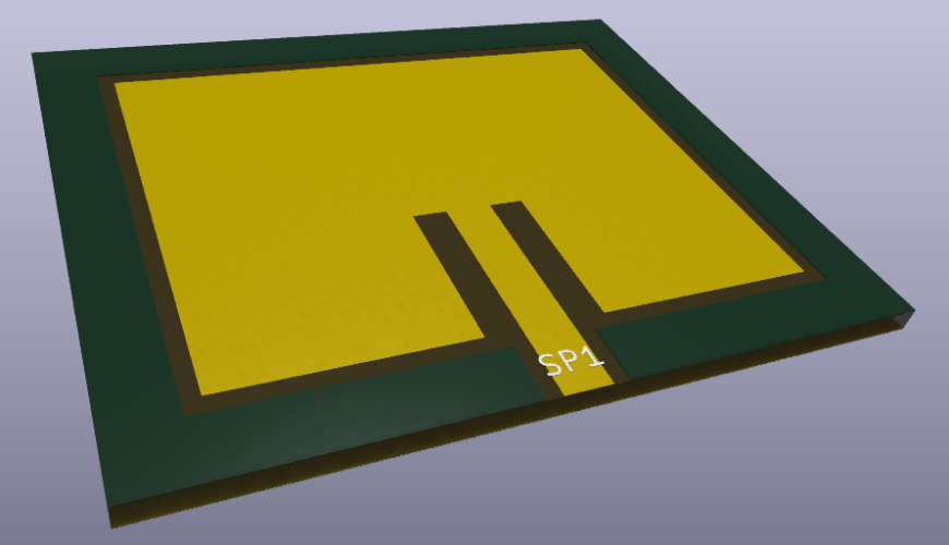
Moreover, the board shall have an SMA connector on each side. The length of the board is going to be 50 mm, and the board will be shared with all other 2 layer designs excluding the antenna, but with proper clearance between the designs to minimize parasitic effects between the designs.
Coplanar waveguide with solid ground plane on the secondary side, two layer board with stitching vias.
Coplanar waveguides are awesome! And they look awesome. And again, designing one for JLCPCB’s process is really simple, as their online impedance calculator supports calculation of CPWs. So the resulting single ended CPW width is 1.77 with a clearance of 0.5mm.
CPWs also need fencing vias. The rule of thumb for fencing vias is that the spacing between the vias orthogonal to the trace (i.e. the space between the vias on each side of the trace) should be less than half the wavelength, and the spacing between the vias parallel to the trace should be less than an eighth of the wavelength.
Given this, we can instead work backwards to what the highest frequency we can support given the restrictions of the manufacturing process.
According to JLCPCB, the smallest via hole for 2 layers is 0.3mm, but it’s a bit small, so let’s go with 0.5mm drill holes instead.
The smallest annular ring will give the minimum distance to the end of the ground plane. Although this probably could be the minimum given distance, it’s always a good idea to give the manufacturer some room, so even though the minimum annular ring is 0.13mm for this process, I will go for 0.2mm.
The minimum distance between vias of the same net is 0.254mm, but again it’s a good idea to give the manufacturer some leeway with these parameters, so let’s go with 0.3mm.
This gives a via gap of 0.3mm parallel to the trace, and 0.2 + 0.5 + 1.77 + 0.5 + 0.2 = 3.17mm orthogonal to the trace.
Putting this into the rules of thumb for the maximum frequency for a CPW gives
3.17mm < λ/2 ->3.17 mm <λ , which corresponds to 52.5 GHz (in this medium, calculated with Saturn PCB toolkit).
For the parallel spacing, we get 0.3mm < λ/8 ->2.4 mm <λ , which corresponds to 66 GHz for this medium. Note, the wavelength is different in different mediums, hence the medium references.
This is way beyond what the substrate can handle, and way beyond my measurement capabilities.
The parameters for the CPW can be seen in table 3.
Table 3. Coplanar waveguide parameters for two layer PCB.
| Parameter | Value |
| Trace width | 1.77 mm |
| Trace to ground spacing (coplanar) | 0.5 mm |
| Via spacing parallel to trace | 0.3 mm* |
| Via spacing orthogonal to the trace | 3.17 mm* |
| Stackup | JLC0216 |
* Since this gives a massive bandwidth, I will give myself some leeway to increase these parameters when designing the board.
Microstrip transmission line with solid ground plane on the inner layer, four layer board
Again, JLCPCB makes it really easy to calculate both coplanar waveguides and transmission lines using their online impedance calculator, and for the microstrip TL we only need to select a single parameter: the stackup.
I normally try to make my designs work with the most standard stackup there is, and in this case the JLC04161H-7628 is their standard four layer stackup.
Using L2 as a reference layer, the dimensions are calculated according to table 4.
Table 4. Four layer microstrip dimensions.
| Parameter | Value |
| Trace width | 0.3493 mm |
| Stackup | JLC7628 |
Coplanar waveguide with solid ground plane on the inner layer, four layer board with stitching vias
With the same stackup as the microstrip transmission line, there is a final parameter to be decided for the coplanar waveguide.
However, since the prepreg layer between L1 and L2 is only 0.2mm thick, using the 0.5mm coplanar ground spacing would result in the ground layer coupling being quite a bit stronger than the coplanar coupling, which sort of defeats the purpose of using coplanar waveguides.
The minimum trace spacing is 3.5 mil, or 0.09mm, for JLCPCB’s 4 layer process, but again there’s no point in using these minimum settings.
Instead, let’s set the spacing to 0.2mm to match the height of the prepreg, which should result in a somewhat equal coupling between the coplanar ground plane and the ground plane on layer 2.
Using 0.2mm spacing yields the parameters shown in table 5.
For the via spacing orthogonal to the trace, we can shrink this since the spacing has changed. Using the same calculation method yields a minimum via spacing of 0.2 + 0.2 + 0.294 + 0.2 + 0.2 = 1.094mm, which is rounded up to 1.1mm.
Table 5. Coplanar waveguide parameters for four layer PCB.
| Parameter | Value |
| Trace width | 0.294 mm |
| Trace to ground spacing (coplanar) | 0.2 mm |
| Via to via spacing parallel to trace | 0.3 mm* |
| Via to via spacing orthogonal to the trace | 1.1 mm* |
| Stackup | JLC7628 |
* Since this gives a massive bandwidth, I will give myself some leeway to increase these parameters when designing the board.
RF via with coplanar waveguide going from primary to secondary side, four layer board with stitching vias
RF vias are tricky to get right, and is sort of the root cause of why I’m doing this project in the first place to be honest. Here is where the theory and simulation (using MoM) have given me the largest difference, so the goal is to try a couple of different sizes. Basically, a classic RF test board.
A via might sound like a simple enough structure, and in general it is. But in actuality there are a lot of parameters going into a via design, especially for a multi layer board. Figure 2 in conjunction with table 6 shows all the parameters that go into a via design.

Table 6. Via parameters explanation in reference to Figure 2.
| Parameter in reference to Figure 2 | Parameter description |
| Tp | Plating thickness |
| T1 = T4 | Outer layer copper thickness |
| T2 = T3 | Inner layer copper thickness |
| H1 = H3 | Prepreg thickness |
| H2 | Core thickness |
| D | Via hole size |
| D via pad | Inner layer via pad diameter |
| D annular ring | Outer layer annular ring diameter |
| D anti-pad | Anti-pad diameter |
As we can see in Figure 2 and Table 6, there are in actuality a lot of parameters going into a via design, and some parameters that have implications to the manufacturing process which must be obliged, such as the via pad diameter and hole size.
Inner via pads/annular rings
The inner via pad, called via pad or inner annular ring (via pad here to separate outer layer annular rings which are absolutely required with inner layer annular rings which aren’t necessarily used), is a topic that suddenly becomes important in RF vias.
There are some discussion into if non-functional inner via pads are useful or not in terms of manufacturability and reliability of the circuit board, none of which I will cover here, but in this context the RF implication of such a pad is more interesting.
So what does an inner via pad mean in an RF via? Well, it can be thought of as a circular stub, which will generate a band stop filter at a wavelength roughly four times the pad copper length (i.e. pad diameter minus the finished hole size).
This is bad, and we do not want that. Moreover, if we think about the impedance of the via itself, assuming all layers have the same copper thickness, the chances of that pad acting as a stub having the same characteristic impedance as the rest of the via is very slim.
So essentially, an inner via pad will act as a non-matched stub. Which is even worse.
Now, it might be possible to trim the impedance of the pad using the anti-pad, but that still leaves a stub. This might be interesting on its own, in trying to use vias as filters, but in the context of just getting an RF signal from the top layer to the bottom layer, via pads just seem to introduce unwanted parasitic behaviors.
So to conclude the inner layer via pad/annular ring discussion, I hope that I have convinced you, on a conceptual level, that I can remove inner pads.
Via impedance
We want to have a characteristic impedance of the via that matches the impedance of the trace going to and from the via, to minimize reflections.
The parameters that will affect via impedance are the antipad diameter, the hole size, the outer layer annular ring size and the plating thickness. So basically every single parameter of the via.
The parameters that we can control, albeit within the manufacturing capabilities, are the antipad diameter, hole size, and annular rings. That leaves the plating thickness which is often decided by the manufacturer, and for a typical 1 oz outer layer, it tends to be in the 15-18µm range, i.e. around 0.5 oz, unless it’s an IPC-6012 process.
Another aspect to keep in mind in regards to the plating thickness is the via aspect ratio, i.e. the hole diameter divided by the height. If the aspect ratio is small, i.e. the hole is small and the height is large, the plating fluid will have more trouble plating the innermost parts of the hole. For a professional process such as JLCPCB I don’t imagine this would be a huge issue, but to give the plating bath a fighting chance, it’s worth considering not choosing the smallest via size and the thickest PCB.
To calculate the actual via impedance is a contentious issue, since it is a 3D issue (or at least 2.5D), which makes it hard. Sierra Circuits has an online via impedance calculator which requires a sign-up to use. It’s free to use though, and in lieu of other calculators, that’s a good place to start.
Notice that I’m saying “a place to start”, because as I said before, via impedance is a contentious issue, and is often solved by simulation, testing and just know-how.
Using Sierra Circuits online calculator as a starting point, I’m starting off with a 0.5mm hole size, with an outer layer annular ring that corresponds to the width of the coplanar waveguide in table 5, no inner via pads and a 0.5mm anti-pad clearance.
A snip of the setup is shown in Figure 3 for reference.

This results in a 40 ohm impedance, and after some tweaking of the antipad to get to 50 ohm, I get the results according to figure 4.

This is all well and good, and I think that it’s an interesting candidate for both simulation and manufacturing, along with using the microstrip transmission lines.
However, the example above does not take return currents into consideration, and is most likely not a good fit for a via with coplanar waveguide out of the box.
I do want to consider the case of the coplanar waveguide though: If we imagine the via as a barrel, with the thickness of 18µm, we can unroll that barrel and tada, we have a transmission line, sort of.
The length of the transmission line is the thickness of the PCB, in this case around 1.6mm, but more importantly the width of the “via transmission line” is defined by the hole diameter, and the spacing to the nearest ground plane can be defined by putting ground vias all around the signal via. See figure 5 for an illustration of this.

With this approach, I think that I can sort of “create” a ground plane around the via itself.
Since the ground vias don’t have any major implication on the impedance of the transmission line going into the via, the placement of the vias are assumed to be only related to the wavelength, as per the CPW calculations above.
Hence, we have some freedom in the placement of the ground vias, within the limits of the manufacturer.
The main limitation to the placement of the vias is the minimum annular ring required, in conjunction with the minimum copper clearance.
So let’s start with the signal via itself.
The clearance between the ground plane and the annular ring should be 0.2mm, but the annular ring needs to be treated differently. From the perspective of the ingoing TL, the annular ring initially looks almost like a power splitter if we’re ignoring the plated hole.
Including the plated hole, it’s a more intricate set of transmission line equivalents. If we also take phase into account, the annular ring should be as small as possible to avoid phase differences at the far ends of the annular ring. I don’t know that this would be a major issue, but it’s at least a confederation worth keeping in mind.
With the minimum clearance between via hole and another trace being 0.254, the annular ring must be at least 0.054 mm in width, but that’s OK since the minimum annular ring has to be at least 0.13mm. Without dwelling too much on this, my gut feeling tells me that there should be as little disruption as possible between the transmission line and the via itself, so for a given via size, the annular ring should align as much as possible to the ingoing TL width. However, seeing as the incoming transmission line for a CPW is 0.294mm, the hole size needs to be less than the CPW width minus the hole size, which for four layers is 0.15mm, leaving 0.144mm for the annular ring, but this is really on the limit of what is practical. So if we instead choose a hole size of at least 0.2mm and an annular ring of 0.2mm to start with, we don’t need to disrupt the process too badly.
JLCPCB’s minimum annular ring size is 0.13mm for vias, and for ground vias since there is a solid pour on the ground plane, this can pretty much be used. That being said, I will design for a 0.2mm annual ring width for the ground vias (note that the annular ring will not be seen, due to the pour, but it’s still a parameter that has to be accounted for).
Given this, we can calculate the “height to the ground plane” as seen from the vias perspective, see figure 6 along with eq. 4.

Now the “via ground plane” will not be solid, which you would normally be a big no, and makes equation 4 kind of pointless, as it calculates the minimum ground distance.
The “real” distance would probably be a function of how many vias there are, along with the distance.
However, if we think about this in terms of how the electrical fields will couple, they will couple to the closest ground reference, and since the ground vias, in a sense, is “coplanar” with the signal via, I think that this could work.
The question then becomes: what of the internal ground planes? Should the internal ground planes be made up of annular rings like the vias, or should it take the structure of an anti-pad? i.e. sort of revolver like or circular, see figure 7.

If I think of the vias as the ground plane, I would go for the left option in figure 7, but if I think of the vias as connecting the ground layers, I would go for the right option in figure 7.
Again, I don’t know what’s the best approach here, but my initial feeling is to go for the left, revolver like option in terms of signal to ground stability. If this turns out to be impossible to manufacture, I think a good solution would be to have an even larger internal annular ring, larger than the “ring of vias”, and have another set of ground vias outside of them.
My reasoning behind this is that for the right option, i.e. an annular ring with a diameter smaller than the “ring of vias” diameter, would introduce a smaller ground gap at the ground planes, which would emphasize the ground clearance being different for the via.
All this talk and thinking leads me back to equation 4, and the reason why I kept it. It’s the smallest gap to the ground reference that sort of decides the impedance of a transmission line.
Given the parameters above, we can calculate the distance between ground reference vias and the signal vias to be
My idea here is simple: if the signal via is a cylinder, then an associated transmission line width would be the circumference of that cylinder. The question then becomes: With a ground reference height of 0.6mm, what width of a 18µm transmission line corresponds to 50 ohms?The circumference is given by the C = D*π, and for the drill size at JLCPCB of 0.3mm the minimum track width is 0.3*π = 0.94mm.
Plugging this into the Saturn PCB toolkit gives us a characteristic impedance of 55.6Ω.
What’s great now is that we can increase the hole size, without impacting the spacing between the vias, to be able to get a transmission line at 50Ω.
With a reference level height at 0.6mm, a transmission line width of 1.135mm gives 50.04Ω using the Saturn PCB toolkit. Working backwards, we can find what diameter hole that is, by dividing the TL width with pi: C = D*π -> D = C/π -> 1.135/π =0.36mm.
To recap, I have made around a million assumptions about RF electronics and how electric fields work, and I have little to no idea what I’m talking about, but I have design parameters for an RF via.
The parameters for the CPW RF via is shown in table 7 with reference parameter in figure 8.

Table 7. Initial values for the coplanar via structure.
| Parameter name | Parameter description | Parameter value |
| D_via_s | Diameter of via hole, signal via | 0.36mm |
| W_AL_s | Width of annular ring for the signal via | 0.2mm |
| W_AP_s | Width of top signal layer antipad | 0.2mm |
| D_AP_ml | Middle layer antipad diameter | >0.6mm |
Note that these parameters should be subject to simulation prior to ordering, which is the reason behind this article. The values shown in table 7 are treated as a starting point which is to be improved upon in simulation, given that the simulation is giving me reasonable results to begin with.
One difference between the via and the TLs is that vias are connected by transmission lines, so I think I’m better off trying to optimize the design against each design tool, to then be able to compare the simulations to reality.