A shallow dive into the different methods that can be used for electromagnetic (EM) simulation, with focus on RF circuit board simulation.
Background
RF design is a tricky beast to tame, and from my experience working with people in the industry, RF board design is almost more of an art than calculation sometimes.
Moreover, most calculations seem to be guidelines rather than hard facts, and the real test is done with actual hardware.
This tends to mostly be due to the quite pronounced parasitic effects that electronic hardware shows at high frequencies.
That being said, designing an inverted-F antenna should not be something that people are discouraged from without using simulation. This article focuses on transmission lines (TLs), vias, RF circuits rather than connecting an antenna to an RFIC. Nothing wrong with that, it’s just that in my experience there are a lot of great resources out there that have already been well tested and documented.
In my case, I’m working on a more complex RF circuit, more specifically a distributed and “cheap” phased array. The project consists of three major parts: antenna, phase shifter and distribution network.
The antenna is just an antenna with 50Ω input impedance, so in general any old antenna would work there.
The phase shifter is a more complex system with multiple RF switches. However, once broken down it’s nothing more than transmission lines that go between switches, all on the same side of the PCB.
The distribution network is in general just a three port power splitter/combiner, so a Wilkinson Power Divider (WPD) is a great choice there, as two of the ports have reasonable isolation.
Where I ran into issues was however in the power divider; I need to route the signal from the primary side to the secondary side of the board. This means a via. But for an RF board designed to work at 2.4 and 5-6GHz it’s not as easy as just using a via.
That’s where simulation comes in. I have been using Advanced Design Systems (ADS) from Keysight for many years, and it truly is a great tool, but it costs a small fortune and is not suitable to tinkerers. I’ve been fortunate enough to have access to ADS, but I am definitely a minority in that regard.
At the same time, I don’t blame Keysight for the steep price of ADS since it’s well maintained and really quite a good piece of software. I’m blown away by the stability of the simulation engine.
However, I’m trying to go towards more open source tools, partly because I like it but also to be able to share my work more easily.
OpenEMS seems to be one of the most used open source EM simulation tools out there, but when starting to dig into the documentation it’s soon clear that it uses a different solver compared to ADS.
And that’s where this article comes into existence: What different methods are there, how are they different and which method is useful in what situation?
Popular EM simulation solver methods
This section attempts to give some background to the problem being solved, and the different methods of solving that problem.
The problem
Electromagnetic fields follow Maxwell’s (or Maxwell-Heaviside) equations which are partial differential equations (PDE) describing how electromagnetic fields are generated by charges, currents and interaction with other fields, and how EM fields affect charges and currents.
An argument can be made that EM fields are what is actually driving the actions in an electric circuit, rather than electrons pushing each other. You might have seen there being a big discussion on youtube a couple of years ago regarding the subject.
In practice it makes little difference, especially for low frequency. But as the frequency increases, the wavelengths shrink and more and more elements start becoming antennas, and capacitive coupling and cross talk become more critical.
So solving Maxwell’s equations becomes more important at high frequencies, as the field couples between elements in a circuit. At low frequencies however, the coupling is so weak that the more classical view of “current being pushed by electrons” is a fair assumption, meaning that SPICE simulation still is valuable and useful, and that any normal layout following a schematic will produce the same result. This becomes less true as the frequency increases.
- Just a comment here, please do still adhere to good layout practices for low frequency. It does not mean that low frequency boards cannot radiate, because there are a lot of sources of noise and coupling can still happen. Keep your analog and digital parts separate, use proper grounding and so on.
I’d like to think it’s due to the impact of the electromagnetic fields at higher frequencies that constitutes the use of EM solvers, leading to the need to solve Maxwell’s equations.
So now I have hopefully made the argument that Maxwell’s equations is what needs to be solved. And herein lies the real challenge with EM simulations: PDEs are really hard to solve.
Pretty much all solvers are numerical solvers using different methods, and I won’t go into too much detail on how to solve differential equations numerically.
From using tools and researching this, there are three main methods that EM simulation tools seem to be using:
- Method of Moments (MoM)
- Finite Element Method (FEM)
- Finite Difference Time Domain (FDTD)
There are essentially three methods of solving Maxwell’s equations, but they differ in their implementation, strengths and weaknesses.
Method of Moments (MoM)
MoM is generally regarded as the hardest to implement, and uses Maxwell’s equations in their integral form, where the integral form relates the fields in a region of space to their boundaries.
Hence, it’s quite straightforward to imagine dividing a circuit up into small elements, and start solving Maxwell’s equations (or the electrical field integral equation (EFIE) ) for each element, which is in a nutshell what MoM is doing.
MoM is closely related to the Boundary Element Method (BEM), and in fact it often uses the BEM method to solve the integral variant of Maxwell’s equations for electric fields (or rather the derived EFIE).
An important note here is in regards to the EFIE, which relates the electric field to the current density. Hence, the equations are solved for charge carriers, i.e. the metal traces. This means that it’s the metal boundaries that need discretizing rather than the entire 3D space.
So what is MoM good at? It sounds like it’s a cure-all for EM simulations since it uses a proven method to solve Maxwell’s equations, and depending on the metal layer layout rather than all 3D space.
Well, for a reasonable approximation to the real world, the element size (or mesh) needs to be small, increasing the number of boundaries for which the equations need to be solved for, and in general it’s preferred for when the surface to volume ratio is small, meaning it’s great for complex and compact structures.
MoM also has a computational advantage compared to the other two methods due to the boundary solver with the surface mesh.
MoM can therefore be used in a lot of use cases, and one of the first use cases was as an antenna simulation tool in NEC. It’s also quite a useful method for complex structures, but requires relatively homogenous materials.
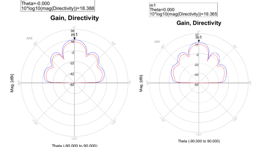
So what does this mean for circuit designs? Well, MoM is an awesome method for anything planar, so if a layout has its RF layout in one layer, or simulating patch antennas. So for most “ordinary” RF circuits this is fine. Going back to the project that sparked this idea, the phased array, both the antenna and the phase shifter boards were simulated using MoM. Generally, MoM works best with thin metal layers, as it often approximates the metal layer to infinitely thin.
One final mention is that there are extended 2.5D and 3D MoM solvers as well, which can do fairly well with vias as well.
Examples of software that uses MoM solvers are:
- Advanced Design Systems (now called PathWave) by Agilent (now Keysight)
- NEC-2, NEC rewritten from FORTRAN to C++. Open source and found here.
- PumaEM, open source and found here. They also included a nice PDF with the theory behind what makes PumaEM tick.
Finite Element Method (FEM)
The Finite Element Method (FEM) uses a 3D mesh, in contrast to MoM, to divide the object into local regions of 3D space and solve Maxwell’s equations for each sub-mesh.
Noteworthy is that the FEM is reused in more applications than just computational electromagnetics, it’s really quite popular for mechanical and fluid dynamics simulations as well, due to its flexibility in geometry and material properties.
Hence, the FEM is quite general, and there are a lot of great resources describing the underlying math (e.g. here), so I will instead focus on what FEM means specifically for solving Maxwell’s equations.
FEM is a more “complete” approach to solving Maxwell’s equations in the sense that fewer assumptions are made regarding the structure of the object being simulated. Moreover, it’s better suited for multi-physics problems where the electromagnetic fields couple to e.g. thermodynamics or other PDE systems.
Since FEM is discretizing, or meshing, all the 3D space that is used within the boundary of the simulation space, the solution space quickly becomes quite large, as all the air and substrates surrounding the charge carrier (i.e. metal) is meshed as well.
So without spending too much time at FEM, as there are so many good general descriptions on how it works, when is it applicable to use for circuit simulations?
Well, as soon as there is a 3D structure present, then FEM really shines. Say for example co-simulating a circuit board with an RF connector, or a metal case, so investigate the coupling between those objects.
In circuit design, there is a case to be made for simulating vias using FEM, at least for higher complexity boards with multiple layers to get a fair approximation of how the via would behave when fabricated.
Examples of software that uses FEM solvers are:
- Advanced Design Systems (now called PathWave) by Agilent (now Keysight)
- ElmerFEM is an open source multi physical FEM solver with a GUI and Python interface.
Finite Difference Time Domain (FDTD)
FDTD is, as the name suggests, a differential solver in the time domain, compared to FEM and MoM, which are solved in the frequency domain.
I like to think about the FDTD as solving Maxwell’s equation straight on, or at least a non-integral form.
In general terms, FDTD works by calculating the discretized form of Maxwell’s equations (using central difference approximations) under the assumption that the space where the equation is solved is small. Kane Yee has a nice lattice model of the approximation here.
The time domain part of FDTD means that the method can solve for a lot of frequencies at the same time, i.e. it’s a wide band solution, while FEM and MoM solve the equation per frequency, meaning that the wider the band being solved for, the more time it would take to solve the equations.
There is however a price to pay for this method, and it’s called numerical dispersion. Essentially, the discretization of the time domain (and somewhat due to the meshing) leads to inaccuracies being accumulated over time. This is generally regarded as the main source of error in an FDTD simulation. To combat this, the grid size and time discretization needs to be quite a bit smaller than one might think.
The error is worse for long time simulations (due to the accumulative error) and high frequency signals (due to the discretization of time being closer to the wavelength).
That might sound like a high price to pay for a simple yet wide band PDE solving method, but there are real use cases outside of EM solvers as well. FDTD has been used to solve the Navier-Stokes equation for fluid dynamics for example.
One of the most highly regarded (or maybe most used) open source EM solvers do however use an FDTD solver, namely OpenEMS, which makes it very attractive for open source enthusiasts such as myself.
One reason why that is, is probably because the FDTD method is quite easy to fundamentally understand, and therefore the easiest to implement (not to say that it’s easy at all, just less hard to grasp than the other two discussed here).
Examples of software using the FDTD method are:
- OpenEMS, widely used and regarded as one of the great pieces of open source software. There is also a project called pyEMS that provides a python interface to OpenEMS.
Comparing the methods
Comparing the theory of operations of the different methods is great and gives some necessary background into where the different methods work better or worse, along with the limitations of each method.
However, it does not provide a good real life use case as to how well the methods work in different scenarios, which is really what I’m after. A practical setup that can help increase the confidence in an RF design.
Therefore, I propose a challenge (for me, no need for you to participate if you don’t want to). The idea is simple: make a couple of designs according to the equations for the elements of those designs (e.g. transmission lines, coplanar waveguide, patch antennas etc.), simulate each design using a tool with each of the different solver methods. Then those designs are manufactured and tested, and we can make a comparison to find which tool was most accurate.
I think it’s important to note that I want to explore the weakness of each method, not necessarily the weakness of each tool, and the goal is to find the best method for the specific job, not the best overall method. Or at least that’s my theory for now, we’ll see once the results are in.
So, the different elements, or components, I want to investigate are:
- Microstrip antenna (e.g. patch antenna), two layer board with a solid ground plane on the secondary side.
- Microstrip transmission line (TL) with solid ground plane on the secondary side, two layer board
- Coplanar waveguide with solid ground plane on the secondary side, two layer board with stitching vias.
- Microstrip transmission line with solid ground plane on the inner layer, four layer board
- Coplanar waveguide with solid ground plane on the inner layer, four layer board with stitching vias
- RF via with coplanar waveguide going from primary to secondary side, four layer board with stitching vias
All components shall have SMA connectors which do not need to be modeled in the simulation (although the FEM could handle it), and shall be measured with S-parameters (with a VNA) or frequency response (with a spectrum analyzer).
Finally, since we are using the associated equations to solve the dimensions of each component, that gives us a chance to also experiment with the limitation of these.
The next post will go into the design parameters of the different elements and components discussed above.