I saw a video on youtube a while back, and inspiration struck: “I could make a smaller version of that!”.
At the time, I was working as a radio firmware engineer on one of the largest semiconductor companies in the world, so naturally the radio part of the hardware I had covered, and knew that it could do this. But this project also scratched my computer vision itch, as it produces an actual image of radio signals.
It should be noted that I’ve already made a similar project at a hackathon at the above-mentioned semiconductor company, but we were using a ruler with some hot-glued copper rods attached at specific points, see image below.
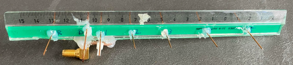
We even tested the gain in the antenna chamber, where the results have been lost to time at this point, but I do remember the gain being around 12 dB.
So the idea here is to remake the results of the video, but with a smaller system. I already have a good idea on how to make the radio part, I’ll just use some of the cheap, low-power radios of my previous employer. But the antenna is the real unknown for me here. Antennas are black magic for me, but I am willing to give it a go.
I will (probably) not be able to test the antenna in an antenna chamber, as I don’t have access to one, and I would like to minimize the number of hardware iterations, which means that simulation is my best bet. I have access to Keysights Advanced Design Systems, which is the simulation software that I used for this.
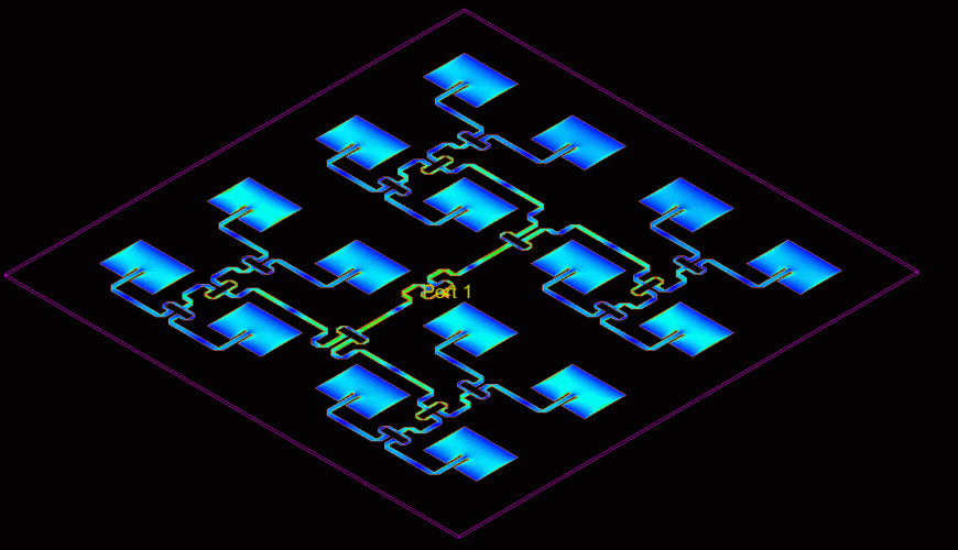
So to the antenna design itself: I have opted for a 4×4 patch array antenna, which is an array of patch antennas fed with a distribution network from a single source.
Designing a patch antenna
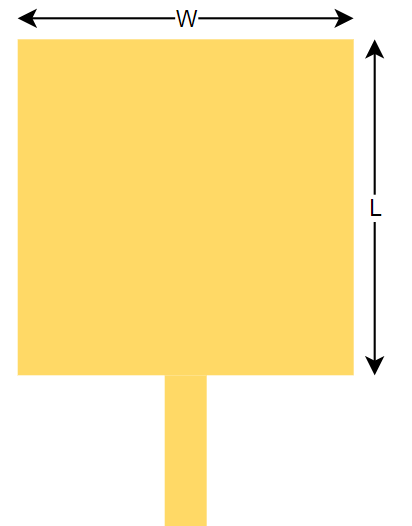
A patch antenna is one of the simpler antenna designs, and has a maximum gain around 6-9 dBi. It’s as its name suggests, a patch which is fed by a single port, on a PCB.
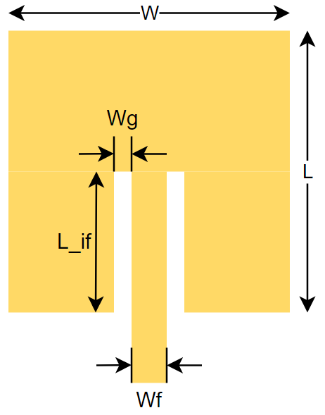
Moreover, to control the input impedance of the antenna, it’s common to use an inset feed, which depending on the inset depth will determine the input impedance.
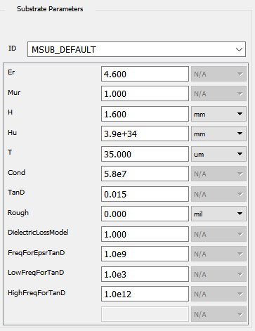
For this design, I will aim for a 50 Ω input impedance and a resonance frequency of 2.45 GHz. The design will be made on a 1.6mm thick FR4 PCB with 35 um copper.
A quick excursion on google yielded a couple of results, which naturally all were different.
There are antenna calculators, e.g. this one or this one, or do-your-own-math examples, along with some youtube tutorials.
To begin with, the antenna calculators both yield the same results: a width of 36.56 mm and a length of 28.18 mm.
However, analyzing the input impedance of these antennas, which is missing the inset feed, yields an input impedance of around 252 Ω, which is a factor 5 higher than the required input. We could make a matching network, but that will take up valuable space on the PCB, so instead an inset feed can be used to match the input impedance. This makes the antenna design a bit more complex however:
With the inset feed antenna, the antenna calculations are:
Where c is the free space velocity of light, f0 is the resonant frequency and εr is the dielectric constant of the FR4. This is incidentally the same equation as for the regular patch antenna, which means that we can re-use the width of 36.56 mm.
From here it gets a bit more complicated, the next step is to calculate the effective permittivity of the substrate, shown in Equation 2.
The εr is 4.6 for OSH park FR4, the height h is the thickness of the substrate, which is determined as 1.6mm, and w is the width of the trace that we just calculated.
You could either put the numbers into the equation, or do like the cool engineers and use the Saturn PCB Toolkit to calculate the effective permittivity, which would give you εreff=4.357.
For the length of the antenna, the following equation are used:
Again, this the same equation as used in the non-inset feed patch antenna, which gave us a length of 28.18 mm. Note that this is a combination of the effective length of the antenna and a length correction factor.
Now, the final piece of the puzzle of the inset feed length and the gap for the inset feed.
The inset feed length, as I understand it, is a method of matching the impedance of a point in the standing wave occurring in the antenna. If the edge impedance was 252 Ω, the center point (at L/2) of the antenna has an impedance of 0 Ω. Using equation 4, the inset length can be calculated.
According to one of the calculator tools, Zin=252, but equation 4 only gives us the input impedance at a given point, and we have to solve that equation in order to find the input impedance of 50 Ω. This paper’s equation 6 has already solved this, but it isn’t too hard to figure out:
Interestingly enough, this seems to be the same point as would have been if we were feeding the patch with a via, according to some sources. This could then lead to an interesting design with the feed network on the secondary side of the PCB. An important factor is then however to keep the ground plane relatively intact on the secondary side, which would be tricky if a via is used, since one would like to feed that via with a signal from a trace, which would of course introduce a slot in the ground plane. However, for a single patch, one could attach an SMA connector on the secondary side.
This leaves us with the inset feed gap and the inset feed line width. From this small thread, this publication, and a few more internet sources, this seems to be a debated topic. The gap in the antenna that the feedline leaves would introduce a parasitic capacitance, and break up the patch. There is some literature on this, for example this one, which claims that the optimum inset depth decreases as the notch width increases, which sounds scary.
However, I will make a couple of assumptions here: I will start with the stripline impedance of the feed line, and then try to calculate the gap. We can calculate the dimensions of a 50 Ω stripline using PCB toolkit, which gives a width of 3.1 mm.
The length of the feedline I have seen should be a quarter wavelength, which makes the length 14.65 mm.
According to Matin and Sayeed, the gap can be calculated with Equation 5.
Using equation 5, the gap width can be calculated to be 0.193 mm. Note that C is meters/mm, F is frequency in GHz, otherwise the result of Equation 5 is silly.
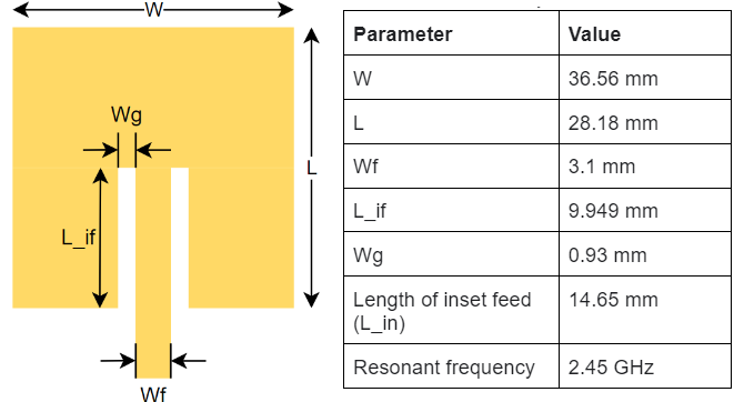
These calculations/evaluations give the following parameters related to the second figure, also shown below for convenience.

| Parameter | Value |
| W | 36.56 mm |
| L | 28.18 mm |
| Wf | 3.1 mm |
| L_if | 9.949 mm |
| Wg | 0.193 mm |
| Length of inset feed (L_in) | 14.65 mm |
| Resonant frequency | 2.45 GHz |
Simulating the designed patch antenna
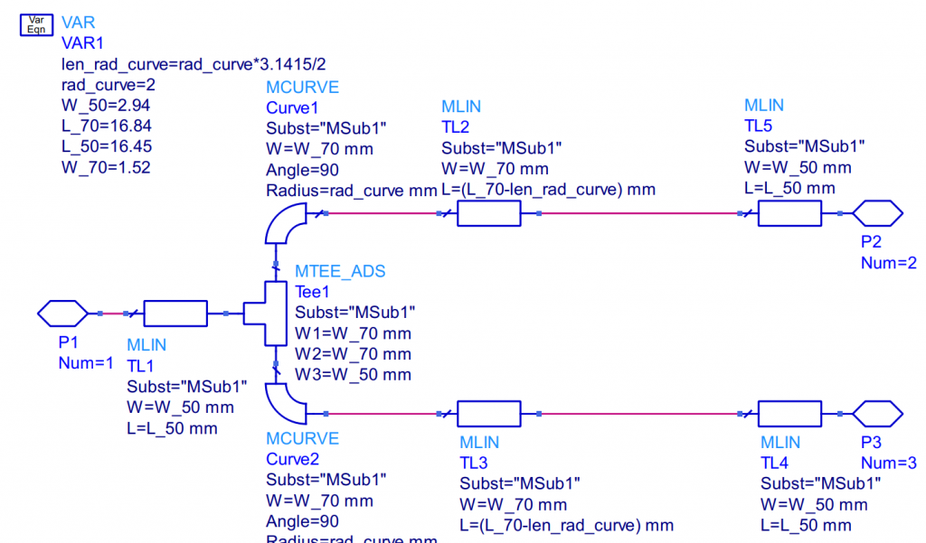
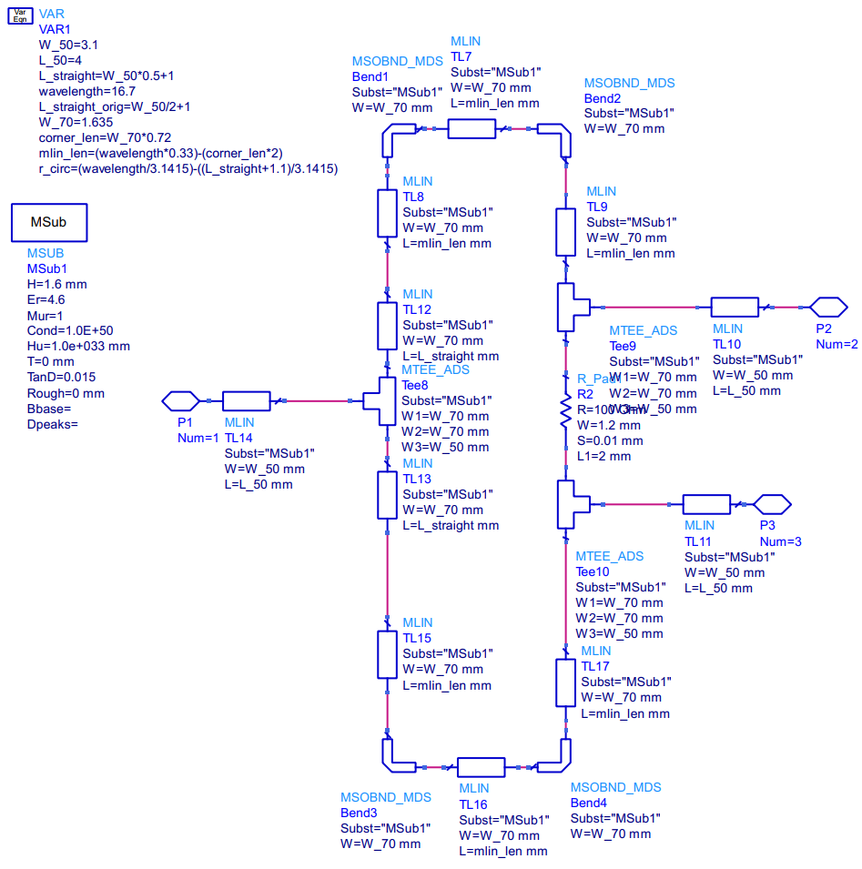
Using ADS, it’s possible to make a schematic using the parameters calculated in the previous section, see the schematic below.
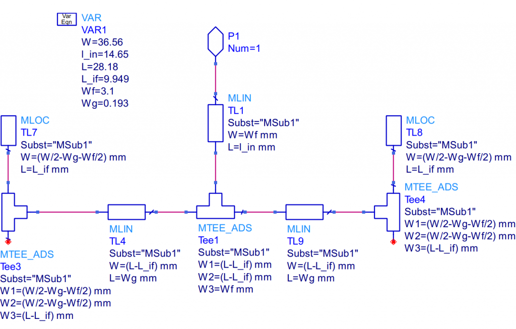
The nice thing about designing a schematic in ADS is that you can easily change the parameters and update the layout quickly. However Tee3 and Tee4 is a bit of a hack, but seems to work with the third port unconnected in the T-junctions.
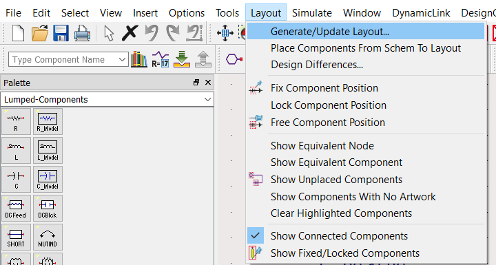
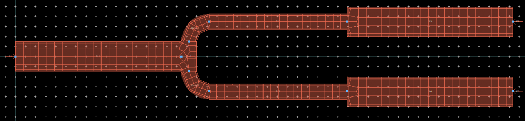
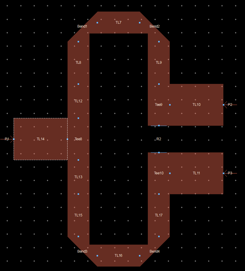
Layout can be generated automatically by using this function in the schematic tool.
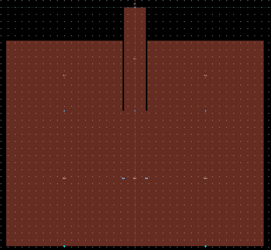
This generates a really nice layout with everything connected:
Making mistakes
Mistakes are common, we are only human after all. At the time of writing this piece, I was on the fourth iteration of the patch antenna, trying to figure out the best approach to simulate.
My mistake was to include the L parameter of an old design (L=29.1589 instead of L=28.18), which introduced an error in both the input resistance (50% error) and the resonant frequency (3% error).
As irritating as this is, they say you learn from your mistakes, and this mistake led me down a rabbit hole of research, checking everything besides the parameters themselves. I picked up some knowledge about momentum simulation, inset feed tuning and antenna tuning in general. Moreover, the error introduced made sense, as the frequency is inversely proportional to the length.
I had already written a 3 page essay on why and how these results could be wrong, but after I changed the length to the correct value, everything looked so much better, so the essay was essentially useless. Anyway, I’ve learned some things, so let’s carry on!
Simulating the antenna
The design is now ready to be simulated. I do not have a license to do FEM analysis, so I have to set up a momentum microwave simulation to try to compensate for this.
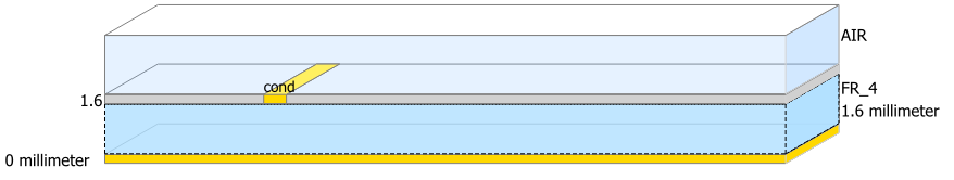
The substrate setup is as follows:
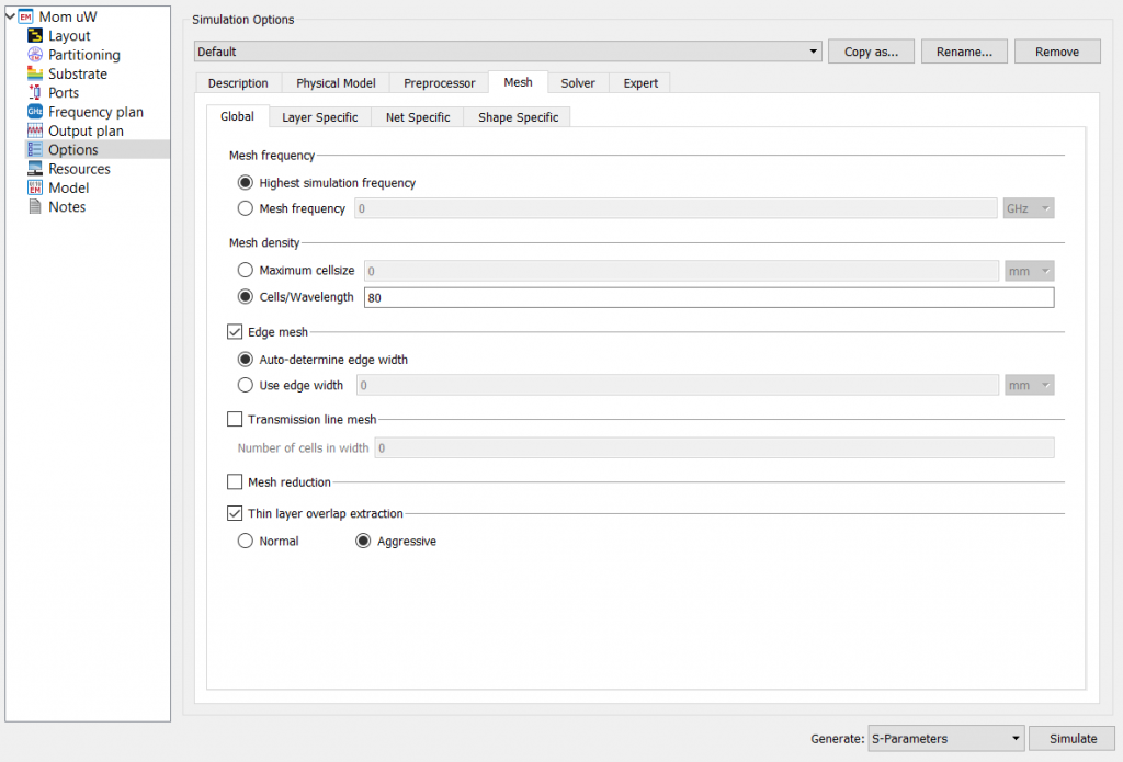
In order to get a more granular simulation, we have to change some settings in Options/Mesh/Global, see image below.
Otherwise, the default settings for Momentum Microwave are used.
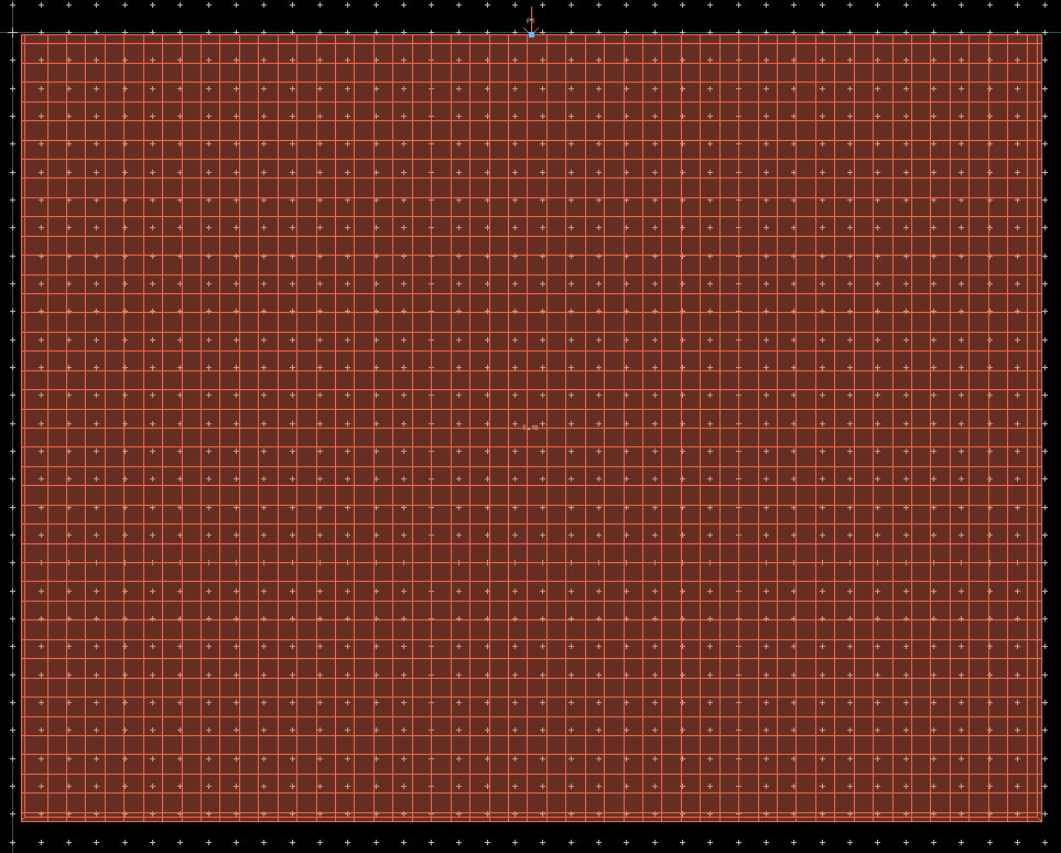
To start with, I simulated the patch only with no inset feed line, see the image below, in order to double check that the calculated parameters make sense.
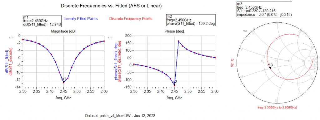
The result of the simulation is shown below, however note that the port and the input impedance are mismatched, so the insertion loss is not optimal due to the reflection at the input to the antenna.
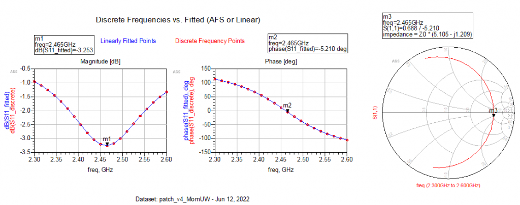
The simulation results reveal that the resonant frequency is 2.465 GHz, which is not far from the wanted center frequency.
According to the Smith chart above, the input impedance is 5.1 times 50 Ω, and according to the online calculator used, the theoretical input impedance is 252 Ω.
Just to try it out, we can adjust the port impedance to 255.25 Ω in the layout port editor just to see if this is the case. Simulation results below.
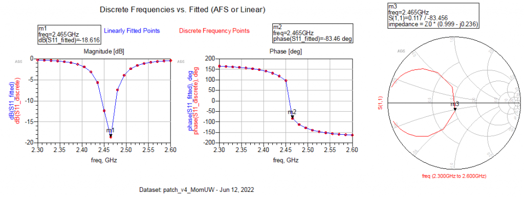
With the impedance matched, it’s clear that the S(1,1) amplitude and phase is corresponding to a patch antenna. The visualization tool shows a very nice standing wave in the patch.
MISSING PICTURE IN ZIP!!!
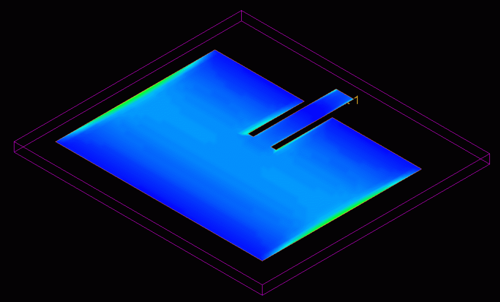
Next step is to simulate the antenna with the inset feed line, so the layout is updated accordingly and the simulation results are shown below.
From the initial simulation results of the entire antenna, we can see that the resonant frequency of the antenna shifted downward a bit, which makes a bit of sense since we’ve introduced a capacitive element with the inset feed line.
According to Figure 4 in this study, the resonant frequency is dependent on the inset feed position, although the variations were less than 1%. Looking at the patch with and without the inset feed line, this corresponds with the simulation results that I’ve found. The above mentioned paper however mentioned that the normal function (see Equation 4) used for inset feed line placement is not optimal, and they suggest a cos4 function instead. Moreover, there seems to be a discussion regarding the distance between the inset feed line and the patch on the side of the feed line, i.e. parameter Wg.
In short, this means that some tuning is required. Looking at the results with the inset feed line, I am quite happy with the resonant frequency, but the inset feed line impedance needs some attention. But first, we need a closer look at the exact center frequency, so for the image below I have reduced the simulation span to [2.4 2.5] GHz.
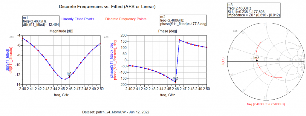
A bit of difference can be seen here where the minima of the insertion loss (2.55 GHz) is not at the real point in the smith chart (2.46 GHz). This is most likely due to the capacitive element between the patch and the feed line.
My first suspicion is that the feed line gap is too small, I’ve seen Wf/10, Wf/20 and Wf/40 as options, and equation 5 was an attempt to find a model for this feed line gap.
So increasing that gap would decrease the capacitance, but also decrease the effective area of the patch.
So to try to characterize this somewhat, let’s increase the Wg to 1 mm, just to see if we can see a difference.
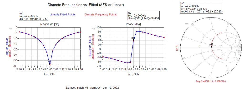
Looking at the results above, it’s almost like choosing 1 mm almost magically worked. Note that the impedance changed drastically, which is the reason why the insertion loss increased. Moreover, the center frequency moved a bit, which also makes sense. However, I think 1 mm is a bit of an over compensation, so from here I will go down a little bit in Wg, trying to find an optimal value. I will spare you all of the simulation results, but I’m basically playing around with the Wg.
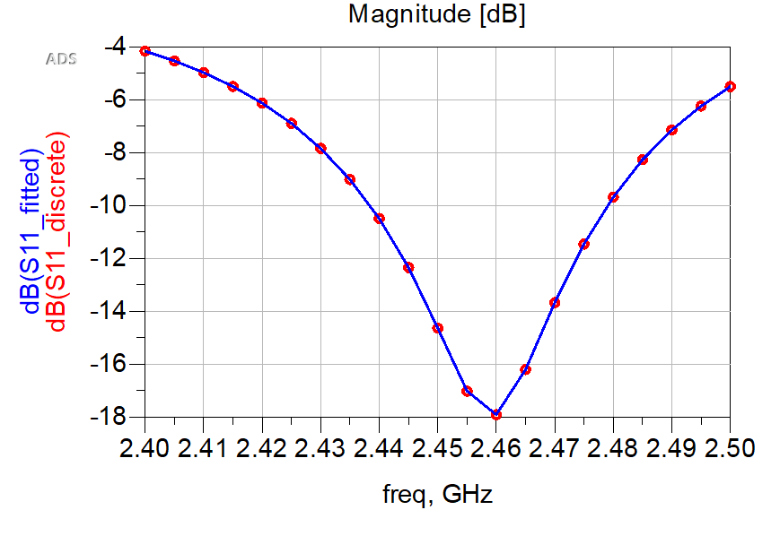
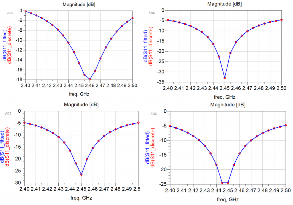
After some simulation (only simulating the center frequency of 2.45 GHz to speed up the process), I found that a gap of 0.93 mm gives me the following result.
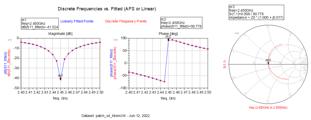
I would say this is a home run. We don’t even have to trim the inset, and we have an insertion loss of -41 dB, a phase of 90 degrees and a slam bang in the middle impedance match.
Regarding the phase shift, I would assume that it’s due to the capacitance, which would introduce a 90 degree phase shift at full tilt. Looking at the EM visualization (see gif below) and the antenna far field visualization, I would say we have designed an antenna!
To recap, the final dimensions of the antenna are shown below.
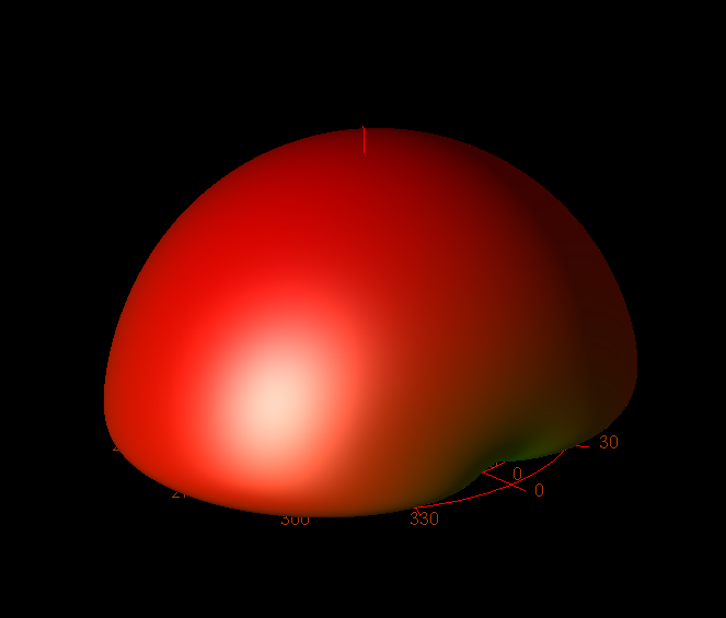
The antenna gain and directivity is shown in the image below.
Distribution network
With the patch antenna done, we have to figure out a way to connect all antennas together. There are two main ways to do this; corporate feed or series feed. There is also the combination of the two, called series-corporate feed, but it’s basically parallel series feeds connected together at the antenna input. Since we have gone through the trouble of making our antenna 50 Ω, it’s not really worth considering series feed.
So corporate feed it is. Not only because it suits the antenna designed in the previous section, but also because the literature points to it having higher gain.
The connection type between the antennas can however look a bit different. I’ve seen examples using wilkinson power dividers or microstrip quarter wavelength matching. Moreover, it’s critical to keep the lengths of the feed lines the same for all patches, to ensure that the antennas are in phase.
I do not know what the optimum method is, so I’ll simulate both options.
Wilkinson power divider
The nice thing about the wilkinson power divider is that all inputs are 50 Ω which makes the scalability easy, but it takes up some space, and needs one discrete component per power divider. A diagram of a Wilkinson power divider is shown below.
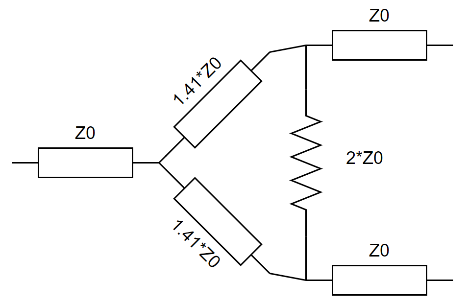
The physical layout of the Wilkinson power divider requires the striplines of the 1.41*Z0 striplines to be quarter of a wavelength of the target frequency. There are also different layout possibilities which I won’t show here, but a quick google image search should show the different possibilities.
To generate the layout, we can reuse the strategy from the patch antenna, by auto generating a layout from the schematic tool. The parameters needed for this are shown in the table below.
| Parameter | Value |
| Width of 50 Ω trace | 3.1 mm |
| Width of 1.41*Z0 = 70.7 Ω trace | 1.635 mm |
| Effective permittivity for 70 ohm trace (used in wavelength calculation) | 3.3043 |
| Wavelength | 67.3155 mm |
| Quarter wavelength | 16.8289 mm |
With these parameters, we can make the schematic. Note that for the resistor in the schematic, I am using “lumped-with artwork”, which will create a pad for us as well.
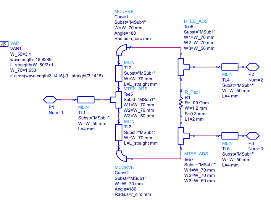
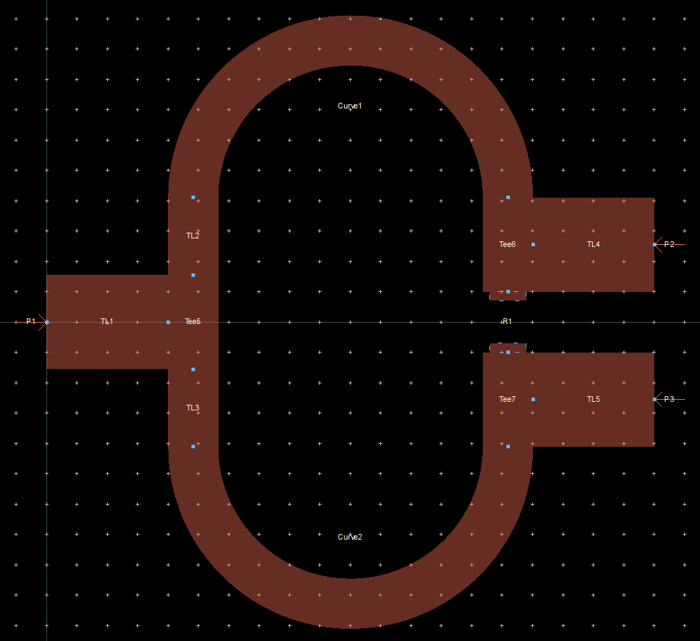
The schematic above is using an 0805 resistor, and will produce the layout shown below.
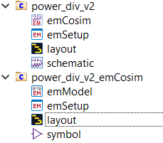
If we now try to simulate this using the same setup as before, it will not work. This is because of the lumped component, which does not simulate in layout simulation. To get around this, an EM Cosimulation setup is needed. This will generate a component and symbol to be simulated in the schematic tool. To set this up, I will reuse the settings from the antenna simulation, but using the EM cosimulation instead.
Once cosimulation is set up, the design is ready to simulate.
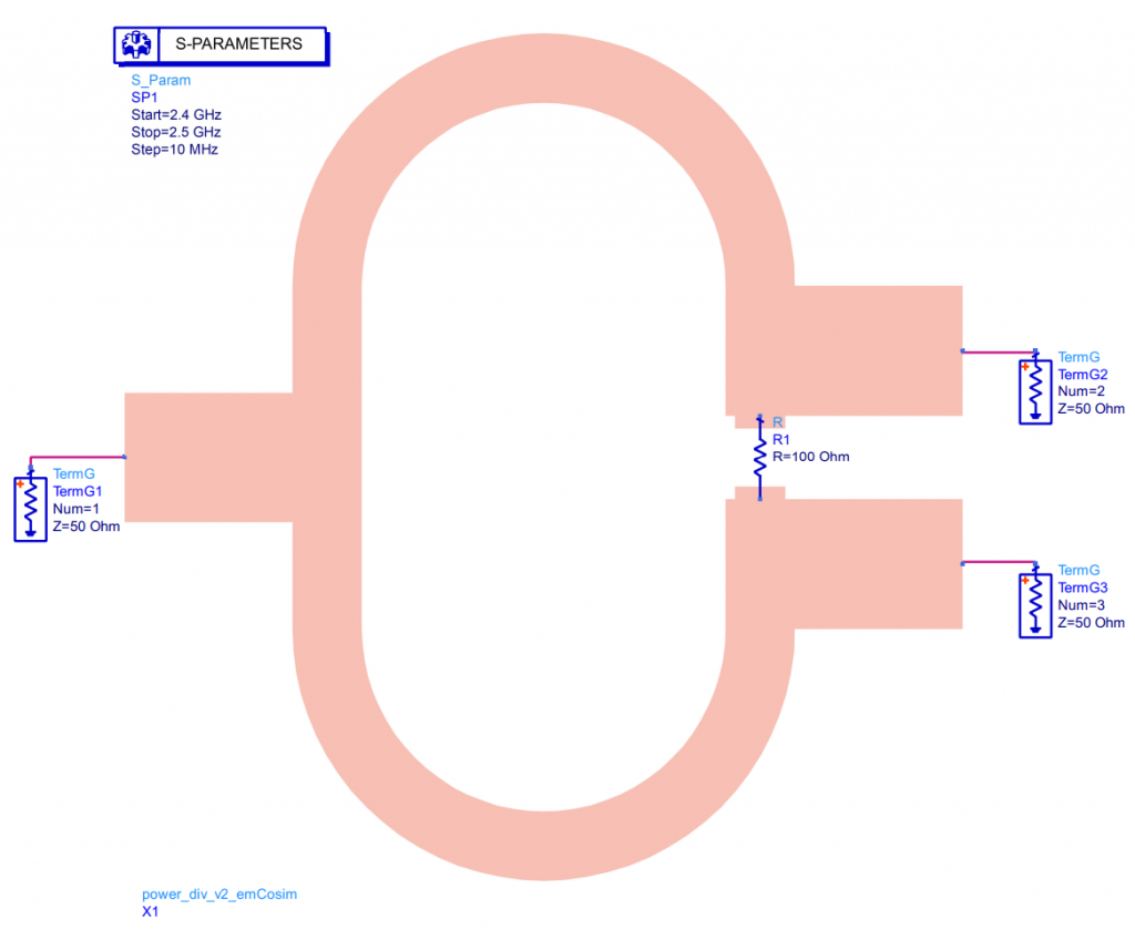
When the simulation is done, a new cell will pop up in the ADS main window, called <cell_name>_emCosim, see image below.
The last step is to create a symbol for the cosimulation layout to be used in the schematic being simulated, which is done by clicking the symbol button in the layout simulation setup window. I recommend using the layout as the source view.
The symbol can then be used in a new schematic to do the simulation. Note: you need to generate the symbol from the coSim layout in order to get the ports for the resistor!
Import the new symbol into a new schematic and attach the S-parameter terminations and 100 Ω resistor, and set up the S-parameter simulation to match the layout simulation:
The initial results are shown below.
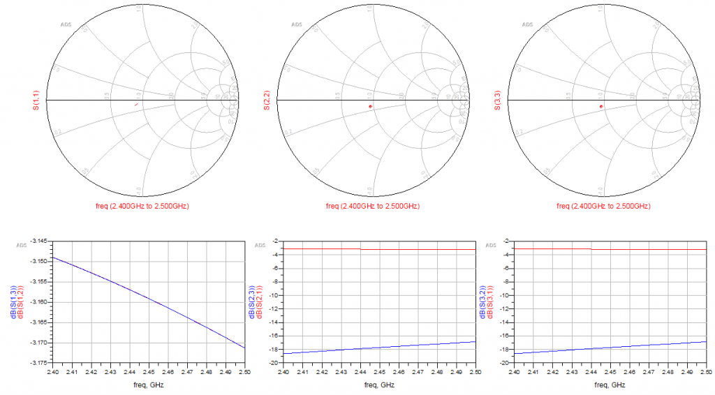
As seen in the results above, we can see that the impedance isn’t a full on home run, but close. Moreover, it’s quite interesting that port 2 and 3 are quite well isolated, with around -18 dB.
Since we know from the antenna simulations that the impedance of the transmissions lines themselves are well behaved (i.e. 50 Ω calculated is pretty much 50 Ω in simulation), my initial thought is that this slight mismatch is due to capacitance.
It could also be a matter of controlling the wavelength. I was a bit surprised that the effective permittivity was so far off the relative permittivity, but I’ve been wrong before. However, to test the effect of this is simply a matter of changing the wavelength in the layout calculations, which is easy to do. So let’s simulate a slightly shorter wavelength of say 16 mm.
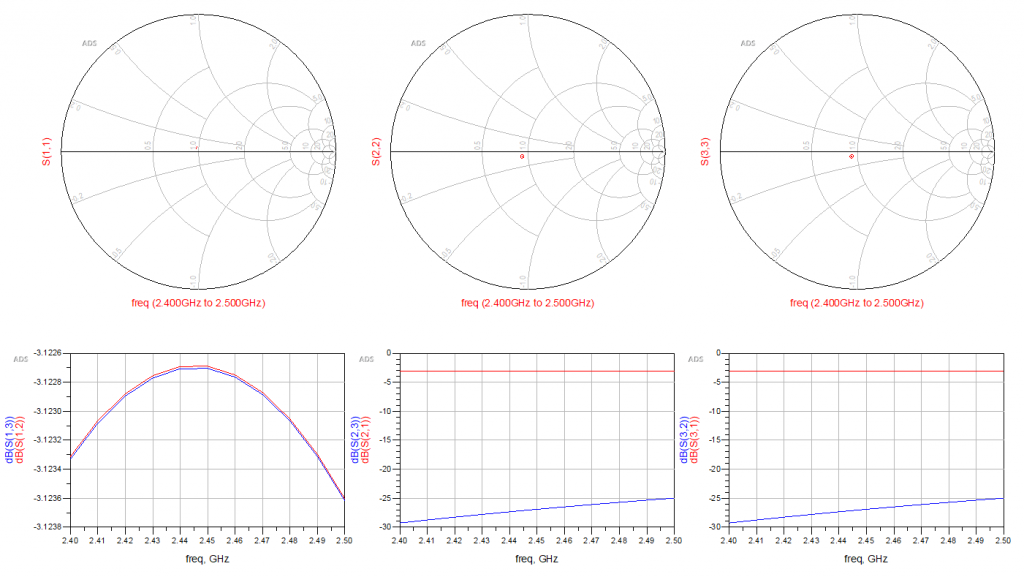
And look at this. A stroke of luck again! I would argue that the peak in the S(1,2) and S(1,3) parameters suggest that we are in the ballpark of tuning the wavelength. I would like to say that the wavelength might not have been the entire issue here, as we’re adding some copper at the end in the T-junctions where the resistor is mounted. These were not a part of the calculation to begin with, but I assumed that the length would be a bit long.
Moreover, a final optimization to remove some parasitics would be to embed the resistor instead of having a dedicated footprint. Fixing that, and some more tuning results in the following result.
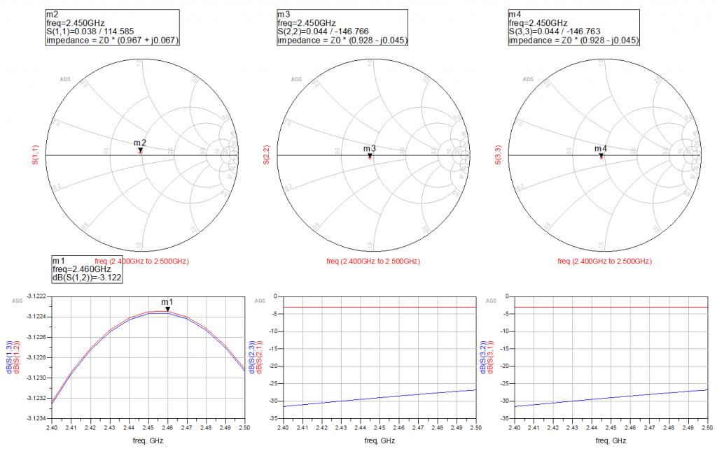
For now, I’m pretty happy with that. The result is not perfect, but then again the production of the PCB will not be perfect either, so this is good enough as a first pass.
At 2.45 GHz, we have an attenuation of -3.1 dB between ports 1-3 and 1-2, and an input impedance of 48.35+3.35j Ω at the input (port 1), and 46.5-2.25j Ω at ports 2 and 3.
Stripline impedance matching
Stripline impedance matching is based on quarter wavelength microstrips, and there is a great guide to this from Keysight. The idea is fairly similar to the Wilkinson power divider, but without the resistor. The Keysight guide is using the LineCalc tool to design this, but I’ve seen that I get slightly different results for the width of the copper trace for 50 Ω compared to the Saturn PCB toolkit. For now though, I’m mostly interested in the length of the trace.
For OSHpark’s two-layer PCB substrate, these are the LineCalc parameters:
The basic idea of the layout is shown in the diagram below.
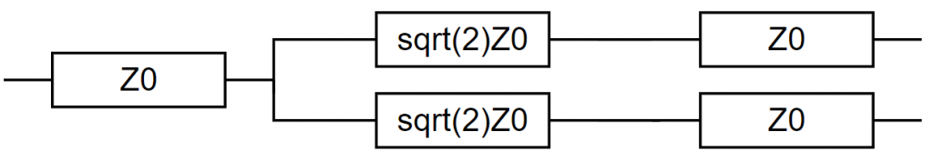
All of the traces shown above are quarter wavelength long. So using LineCalc and PCB toolkit to calculate these, I get the following:
| Parameter | LineCalc result | PCB toolkit result |
| Width, 50 Ω | 2.94 mm | 3.1 mm |
| Width, 70.7 Ω | 1.52 mm | 1.6 mm |
| Length /4, 70 Ω | 16.93 mm | 16.45 mm |
Starting with the LineCalc results, we can set up the following schematic in order to make an automated layout.
The above schematic generates the following layout:
Now, for the simulation results, we can see something interesting.
An interesting observation can be made here: This is basically a Wilkinson power divider but without the discrete component. And all of a sudden we have a lot of reflections on the outputs (port 2 and 3). The input looks great, but the output suffers from reflection, which isn’t nice and it reduces the efficiency.
However, put a 100 ohm resistor between port 2 and 3, and you have a wilkinson power divider! I think it’s clear that the Wilkinson power divider is the best option for this application, so after some tweaking of the parameters, this is what I end up with.
You might have noticed a change in the look of the layout here. The main reason is that the mesh calculation isn’t really that good in ADS; it doesn’t follow the curve, instead it breaks the corner down into small pieces. Therefore, the length is always smaller than what is expected, which is not the case in the real world. So I changed to corners instead, which made the mesh fit the layout better, and it was a bit easier to tune.
I played around a bit with the mesh size, increasing the frequency for which the mesh is made, which made a big difference in the round shape, but not really for the square one shown above. I ended up with the following simulation results:
The input and output impedances are OK matched which hopefully should minimize the reflections. I have a loss between the inputs and outputs of ~3dB, which is near enough perfect, if you think about the power being distributed equally between the two ports, meaning the power at one of the ports is half of the input power, i.e. -3 dB.
I would like to note here that there most likely is a third option: an integrated RF splitter IC, such as the BP2U1+ from Minicircuits. Moreover, it would be a neat project to try to make this type of antenna using chip antennas with integrated splitters as dividers. I haven’t looked into this, but if it doesn’t exist there is maybe a good reason for that. Otherwise I’ll come back to that. But regarding the power divider, since we’re trying to simulate the entire patch array, I will use the stripline method.
With the Wilkinson power divider now done, it’s time to put the patch antenna and the power divider together.
Putting it all together
I’m down to the last variables, which is putting it all together, hoping that it all fits, and doing the last pieces of tuning.
The plan is to attach two patches together with the Wilkinson power divider, and then connect two of those to another pair with a Wilkinson power divider etc. See the image below for a diagram.
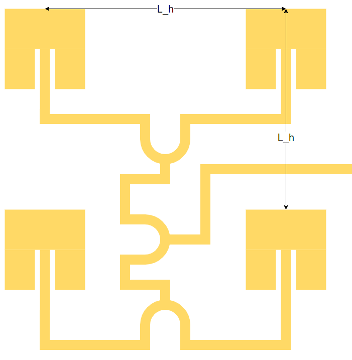
The distance between the patches needs to be controlled, where the aim is to receive as high directional gain as possible. According to this article from Analog Devices, a typical spacing is half of the wavelength spacing between the element centers. Moreover, the wavelength here is referring to the free space wavelength, i.e. 12.24 cm for 2.45 GHz.
Following the schematic above, we can use the earlier schematics to make a model. The Wilkinson power dividers and antennas are connected with 50 Ω transmission lines, with lines calculated such that the distance both horizontally and vertically is half a wavelength.
Since the size of the schematic is getting a bit ridiculous right now, I’ll only show the generated layout. I’m still using the schematic tool to generate the layout for this, as it’s easy to tweak parameters, should (or rather when) it be needed.
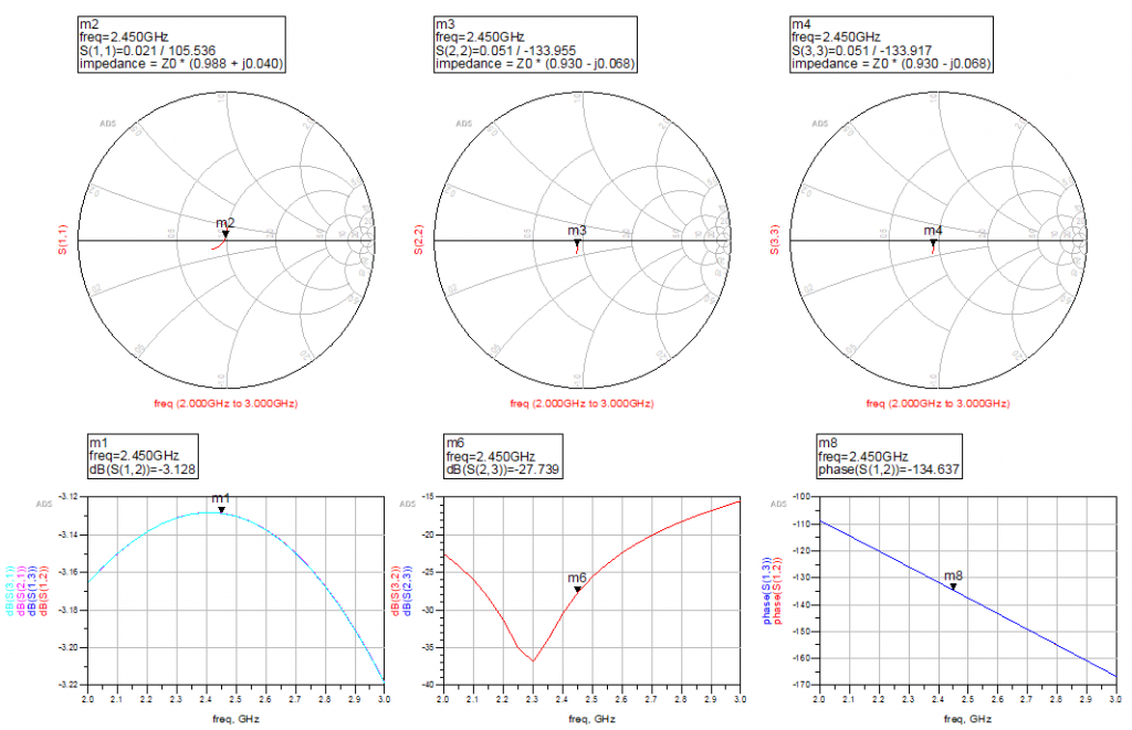
As a first pass, I simulated the four patches without the resistor in the wilkinson power dividers, just as a test to see if the center frequency was maintained.
Mainly because it’s cool, but also as a check, I plotted the waves in the Momentum Visualization tool, see gif below.
The antenna gain is shown in the image below.
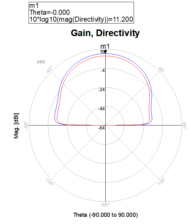
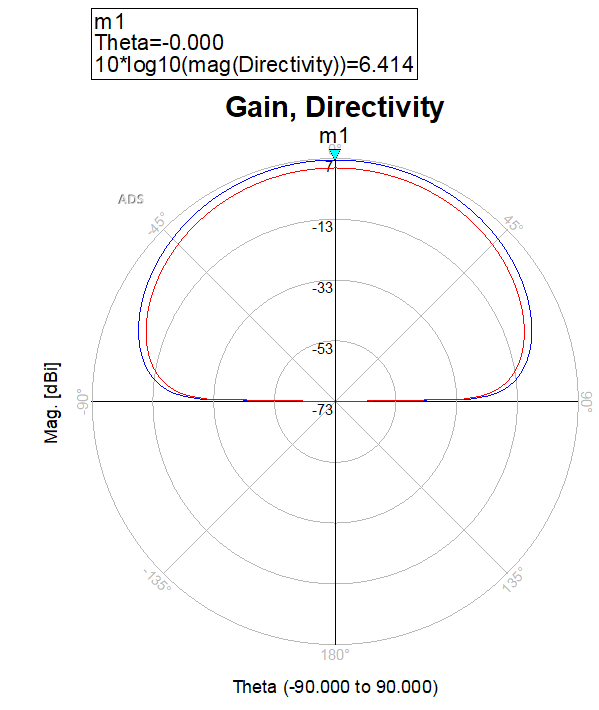
Note that there is indeed an increase in directivity, where one patch produced a simulated maximum directivity of 6.4 dB, the 2×2 patch antenna array has a simulated maximum directivity of 11.2 dB.
So let’s get into the tweaking shall we? As we have our baseline, we should go from here.
From a practical point of view, I’d like to investigate the impact of shortening the antenna feed line a bit (not the input to the antenna, but the length of the actual trace), as it’s a bit tight where the three power dividers are located. For future me, it might be a good idea to look into a 1-4 power divider instead, but we have what we have for now.
Moreover, I’ve seen some literature and discussion regarding the spacing between the antenna elements, and how that affects the antenna parameter.
Looking at the literature mentioned above, increased spacing isn’t such a bad idea for directivity, which is what we’re going for here. To test this, I simulated the same 2×2 setup for 0.5λ (results above), 0.6λ, 0.7λ and 0.75λ. This is why I’ve opted to use the schematic tool, as I only need to change one number instead of recalculating the lengths of each stripline.
However, at this stage, the simulations take quite a while and makes my ultrabook quite toasty, so even if I save time in generating the layout, the simulation time is up in the 10 minute range. Although, that is small potatoes (poorly translated swedish saying) compared to the overnight simulations we made back at Uni.
Anyhow, the simulation results are shown below.
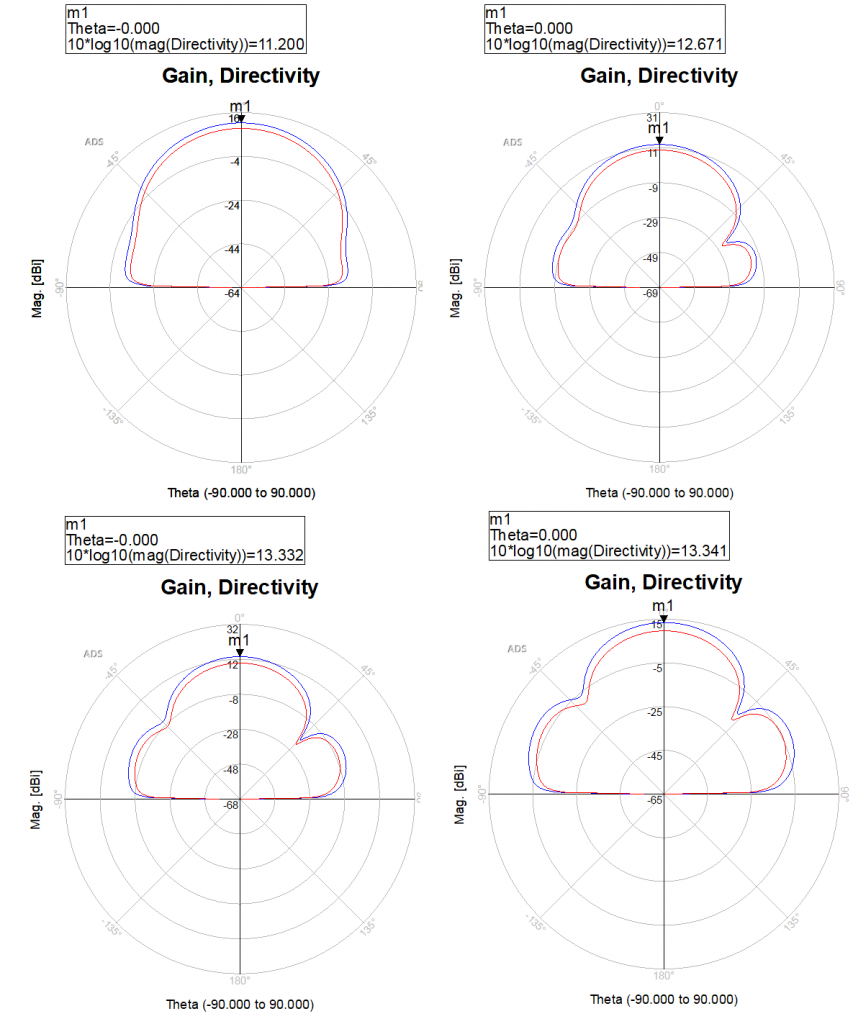
What is interesting, I think, is that the input reflection is affected by the increased spacing. I would assume that it would be affected much for the first few iterations, as the power divider was quite near the radiating elements. But it seemed to move downwards for each iteration, which was a bit surprising to be honest.
Moreover, I thought it was very cool seeing the side lobes of the antenna start appearing in the larger spacings. It was also visible in the 3D far-field visualization, but I didn’t include it here, as I already have a lot of images.
So which spacing should you choose? In my mind, the gain from 0.7 to 0.75 λ isn’t that great, which seems to correspond to the literature as well. I gain ~0.6 dB going from 0.6 to 0.7 λ, but the input reflection is less for 0.6λ.
That being said, I have done these simulations without the resistors in the Wilkinson power dividers, so I would suspect these being lower in actuality.
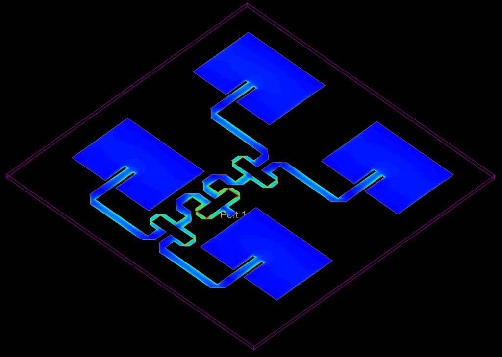
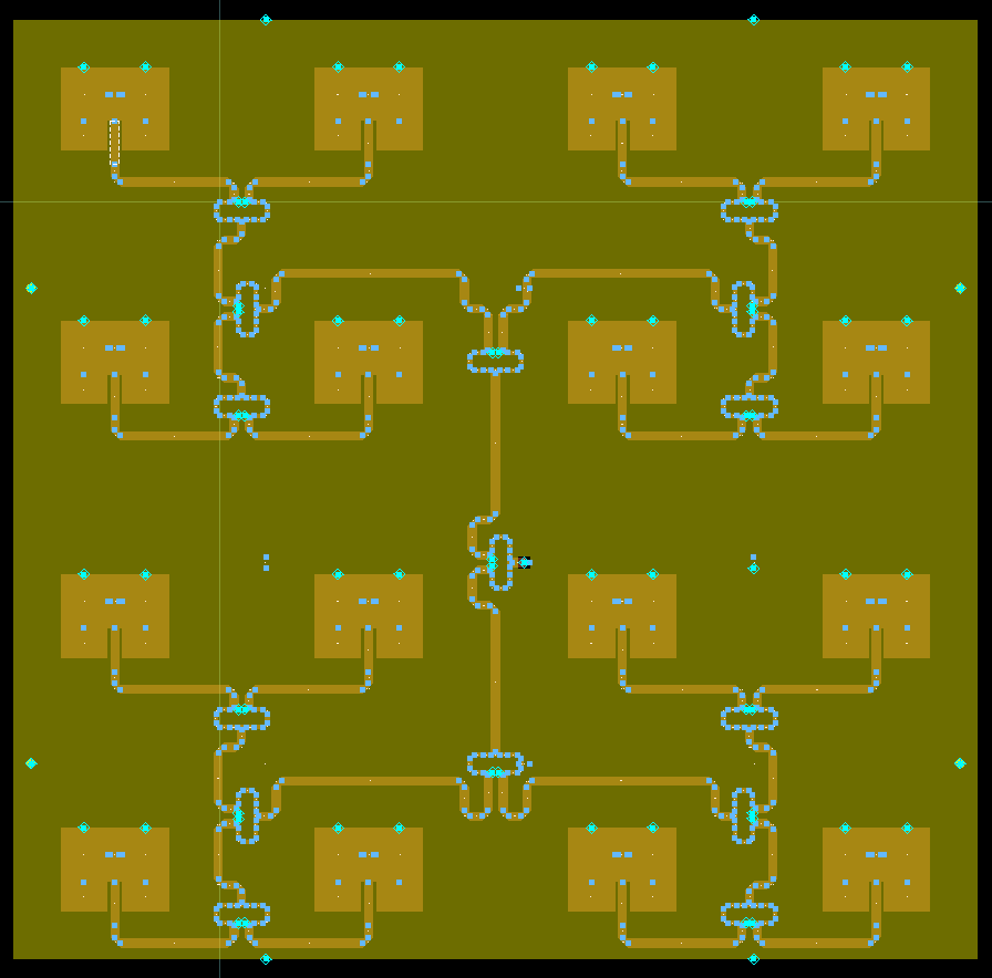
For the aim here, I am going to go with 0.7λ to get that extra 0.6 dB gain, but I do want to redo that simulation for the full 4×4 array, just as a double check. And believe or not, I’m at the stage where I can actually make the full 4×4 array!
Again, the schematic is a bit silly, see below. I am not even able to see the whole thing without ADS blurring the details. I mean, look at the image below.
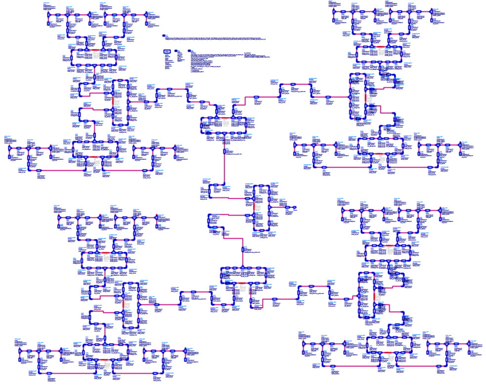
This produces a layout that looks like this:
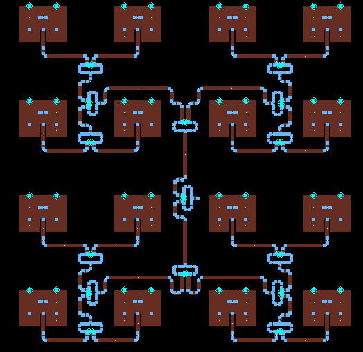
Note that I had to do a couple of squiggly (correct engineering term) lines in order for the traces to have matched length, but not collide into each other.
I think it’s fair to say, this will be a monstrous simulation. Just calculating the mesh took a minute. The simulation ended up at approximately 3 hours, so I spent some time making sure that the setup was OK before starting the simulation.
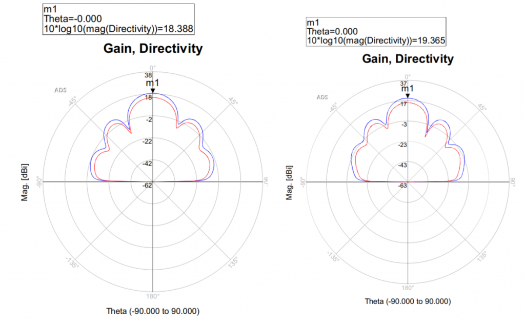
The final results for directivity and gain are shown below.
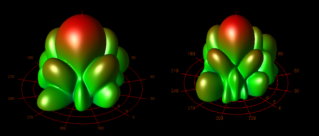
The antenna 3D view is shown below.
A gif of the standing waves can be seen below.
The far field cut tool is reporting the following max gain for the two antennas:
| Antenna spacing | 0.6λ | 0.7λ |
| Max gain | 14.489 dBi | 14.840 dBi |
| Max Directivity | 18.427 dB | 19.365 dB |
The scale on the gain and directivity plots are quite large, making the gain look larger than what it is. But it’s clear that both antennas work quite nicely in my opinion. It might not be the insane gain that I had maybe hoped for, but note that the Wilkinson power dividers were not using the resistors between port 2 and 3, which in my mind would affect gain a bit.
The real test is however the manufactured antenna, and the design is almost complete, it’s missing an SMA connector and board outline.
The board outline is important in order for the antennas to radiate as intended, and it needs to be extended by at least 6 times the height of the substrate, in our case 9.6mm. To have some margin, I will extend the ground plane a bit more, also to have mounting holes for support structures.
I intend to place the SMA connector on the secondary side of the PCB, and to minimize stub length I have opted for a vertically mounted through hole SMA connector which connects to the ground plane on the secondary side, and has the feedline come through a hole in the PCB at the port location. However, it’s kind of hard to find an SMA connector with a through hole mount without supporting legs, which I cannot use as the legs would be in the way of the power divider. Another alternative is to go with a surface mount SMA connector, but then I would need to control the via properties. Having a quick think about this, I think the best solution is to mod a through hole mount SMA connector, removing the supporting legs and solder the shortened legs on the secondary side of the PCB, and the pin sticking through a hole in the PCB and soldered to a pad on the primary side. The hole is then a non-plated through hole, but with a pad on the primary side, and a bit of clearing on the.
The pin size for the SMA connector is 1.27 mm, and the center hole size is 1.5 mm as per the recommended mounting hole dimensions.
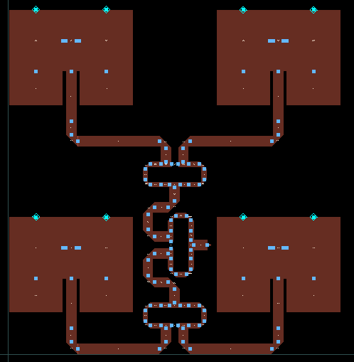
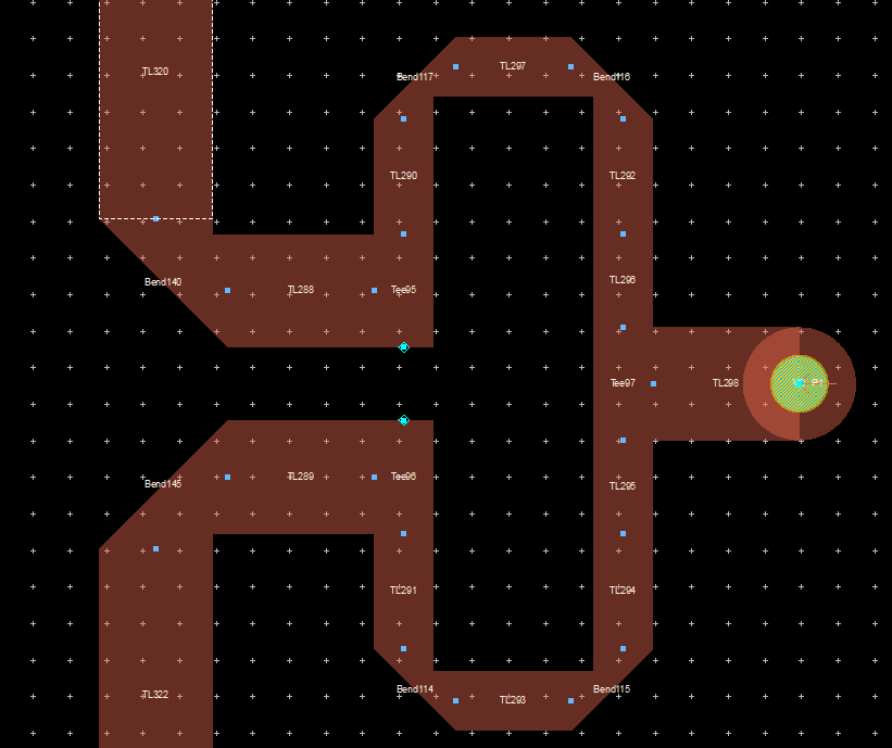
The mounting holes I have made are 3 mm in diameter, which then should accept a jig should I need it. The layout ready for manufacturing is shown below.
One final time then, let’s simulate the antenna again, using the final layout. Note that this is then using a non-ideal ground plane, which should affect the parameters.
The negative side of port one is now feeding the ground plane where the SMA connector is connected. The gerber files and ADS workspace can be found on my GitHub.
Ordering the real antenna
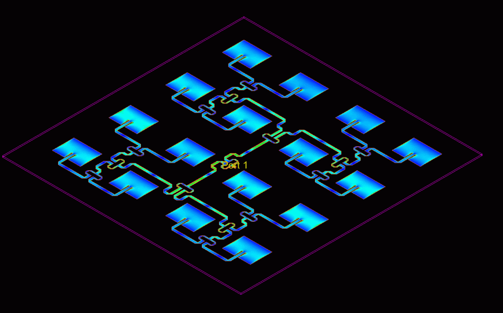
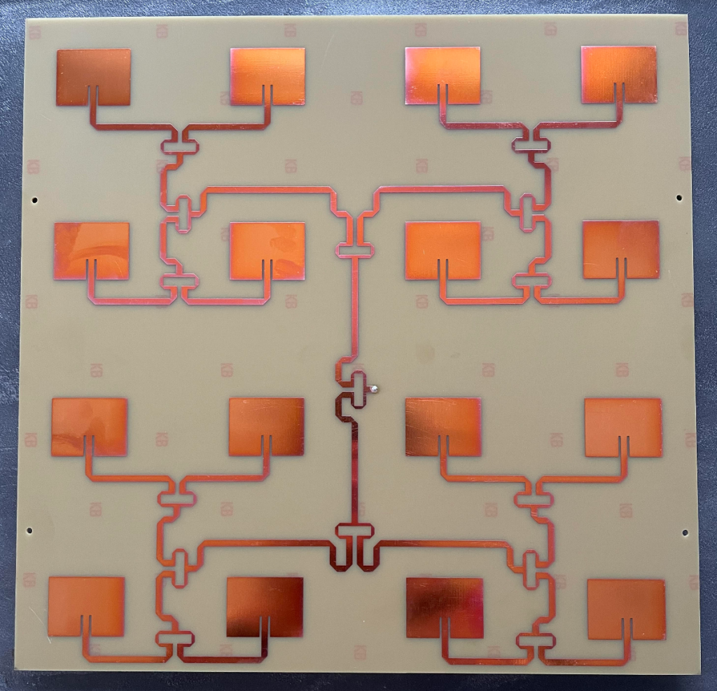
I ended up using PCBway instead of OSHpark, mainly due to price. OSHpark is in general a very good manufacturer, but the antenna ended up much larger than anticipated, it’s approximately 30x30cm. Moreover, the dielectric that OSHpark and PCBway uses are pretty much interchangeable, so it shouldn’t have an impact on quality. I ended up ordering 5 antennas for ~$250, and the result can be seen in the image below, and looks pretty cool if you ask me.
I had some female SMA connectors laying around, from which I snipped off the legs and soldered to the backside. The soldering here is a real bodge-job, so I’m sorry in advance. The main reason is that the SMA ground connects to a massive ground plane on the backside, which is a real thermal sink. Luckily I had access to both hot air and soldering iron, and I don’t think it would have been possible to solder this without both. So using four hands, I heated the backside and SMA connector with the hot air, and soldered using the soldering iron. Below you can see my sorry excuse for a soldering job.
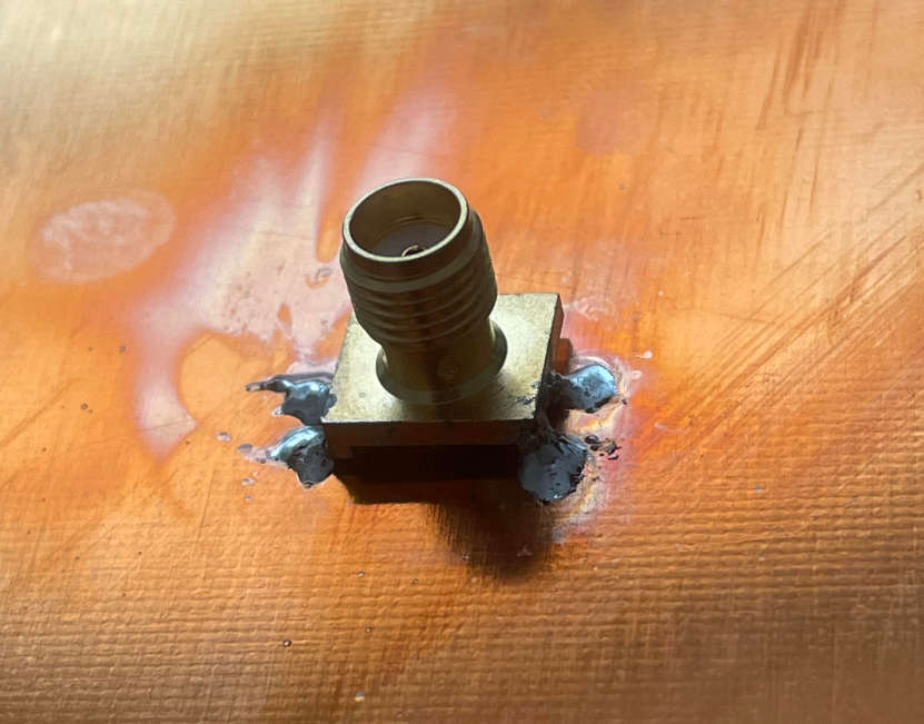
But at least it’s on there now.
The final job is soldering the 100 ohm resistors to the Wilkinson power dividers. I’m unsure if 0805 resistors will fit in the space, as the spacing between the output terminals is 2mm, and the length of an 0805 resistor is also 2mm. But just to be sure, I also ordered 1206 resistors.
However, I am interested in testing the antenna with and without the resistors soldered on there, just to see if my thesis that it affects gain is correct. That leads us into testing the antennas.
Testing the antennas
The best way to test antenna parameters would be to have an anechoic chamber. But those are heavy, and expensive, and take up a lot of room, and the only one I have somewhat access to is currently not working. So, that leaves me with testing the antenna myself.
I had a chat with a good friend of mine who works with antennas for Ericsson in Sweden, so it’s safe to assume that he knows his way around testing antennas. He suggested testing it outside, to minimize reflections. I have access to the roof on my apartment building, which isn’t ideal since it’s in the central area of Oslo, but since I don’t really have much of a choice, that’s what I will have to go with.
So to test the gain of the antenna, I will have to compare the measured RSSI for the same setup as an antenna with known gain. It’s far from ideal, but I have little choice. If I have access to an antenna chamber in the future, it would be cool to test this. And if you, the reader, happens to have an antenna chamber and is willing to try this, please leave a comment and we could maybe make something happen.
Testing antenna gain
To test the antenna gain at home, I have to cut some corners. I have an antenna from a Jetson TX2 platform, which is an omnidirectional WiFi antenna, which according to the Jetson TX1 and TX2 OEM Wireless Compliance Guide has a peak gain of 2.81 dBi at 2.44 GHz (values from Table 2).
The antenna that comes with the Jetson TX2 developer kit is a Pulse Electronics W1043 blade antenna, and according to the datasheet, the average gain in the XY plane is 1.03 dBi at 2500 MHz, and a peak gain of 2.65 dBi. One slightly annoying thing about these antennas however, are that the interface is using a normal SMA male connector, but missing the pin. I have had this issue before, so I just took a regular pin from a header connector, cut that to size and put it in there. I’m aware that this isn’t the best way to do this, but I would argue that I have made approximations in my test setup that most likely is affecting the measurement more than this. So if we lose a dB due to this, it’s well within the range of uncertainty. Otherwise, the system was kept as similar as possible between the two antenna setups – with the same length of cable.
So which value should I use? It differs a few dB between peak gain and average gain from 2.4 to 2.5 GHz, but seeing as we don’t know the exact which point the maximum gain is, I’m inclined to use the average gain. Moreover, the best way would be to rotate the W1043 antenna and take measurements for each measurement.
So why do I care about this antenna? I plan to use this as a reference antenna to perform the gain measurement. To do this, I need to take care to keep the center of my patch antenna array in the XY plane of the W1043 antenna. So my plan is to use the follow test setup:
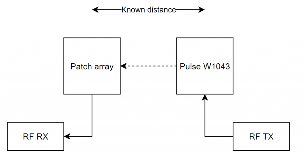
For the RF RX and RF TX, I plan to use the CC1352P-2 LaunchPad from Texas Instruments. It’s a really neat tool that I’ve used quite extensively. It has support for both 2.4GHz and sub-1-G bands, but for this I am using only the 2.4 GHz part of the radio. The idea here is to first make a reference measurement using two of the Pulse W1043 antennas, sweeping from 2400 to 2480 MHz, measuring the RSSI at a set distance. Assuming that the orientation of the antenna isn’t affecting the gain too much, I only need to do this with the antennas oriented in the XY plane to each other. I then need to correct for the different average gain of these antennas, giving me a reference measurement with an antenna with a known gain. Noteworthy here is that I will most likely have multipath, but I will try to minimize that by minimizing the structures near the measurement. The distance between the antennas needs to be large enough to be in the far field/Fraunhofer region, which according to this article, is given by equation 6 below.
D is the largest radiating element of the antenna, and is the wavelength. Using the approximation that the antenna is 40 cm and the wavelength is 12.5 cm, this gives me.
To ensure that the distance isn’t too near the limit of the far field, I set the distance between the antennas to 3 meters.
When the RSSI between the reference antennas has been measured, I can switch out one of the Pulse W1043 antennas to my own antenna design and compare.
Since I cannot control the multipath, I think it would be hard to measure the lobe pattern, but I will try. The aim is to measure the RSSI with the patch antenna array pointed in different directions, sweeping the frequency range for each measurement. But the really interesting measurement is straight on.
I will also have to control the transmitted power of the CC1352P to ensure that the RX is not in saturation. I will however have to tune that parameter when performing the test.
When I have my measurements, I should be able to compare the gain in each direction to the reference measurement, and simply calculate how many extra dB’s I got (if any) in each direction compared to the reference measurement. The reference measurement is assumed to be omnidirectional.
For the data acquisition part, I’m simply using a python script to control the two CC1352P boards via UART, and then saving the data to a CSV file. The code can be found on my GitHub. I’m using code composer studio 11.2 from TI with the SimpleLink CC13xx and 26xx SDK 6.10, and basing the code on the UART and packet RX/TX examples.
Note that the CC1352P launchpads need a cap resoldering before external antennas can be used.
When the weather in Oslo had a pause between rain storms, I headed up to the roof terrace of my apartment building early one Saturday to not spook the other tenants, and set up my antenna measurements. See the images below for the setup.

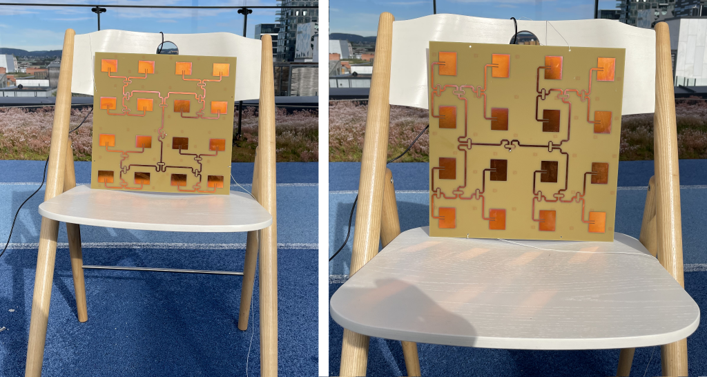
The setup is far from ideal, as there is a lot of concrete and metal around, but I figured it’s slightly better than inside my apartment. I also turned off WiFi and Bluetooth on my phone and computer during the measurements, to not influence the measurements too much. I do expect the results to be quite noisy as well, but I hope I can draw a couple of conclusions from this test at least.
Antenna test results
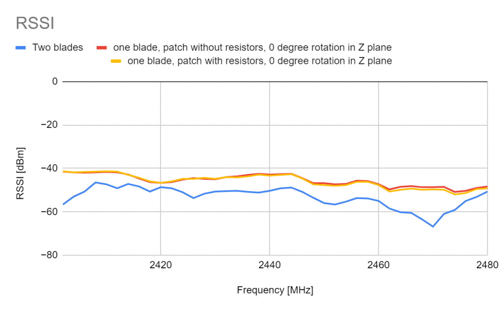
So with the setup shown in the last chapter, I did three measurements per test, which were:
- Two blade antennas (reference measurement)
- One blade antenna, one patch array antenna without the resistors for the Wilkinson power dividers, 0 degree rotation in the Z plane
- One blade antenna, one patch array antenna without the resistors for the Wilkinson power dividers, 90 degree rotation in the Z plane
- One blade antenna, one patch array antenna with the resistors mounted for the Wilkinson power dividers, 0 degree rotation in the Z plane
- One blade antenna, one patch array antenna with the resistors mounted for the Wilkinson power dividers, 90 degree rotation in the Z plane
I also repeated the measurements where I transmitted either from the blade antenna, or the patch antenna. The RSSI measurements are shown below, only for the 0 degree rotation, as the loss in RSSI at 90 degrees was ~-14 dB. The results of the transmission from blade and patch antenna are concatenated, to average 6 runs per measurement.
The difference in RSSI increase is shown in the figure below.
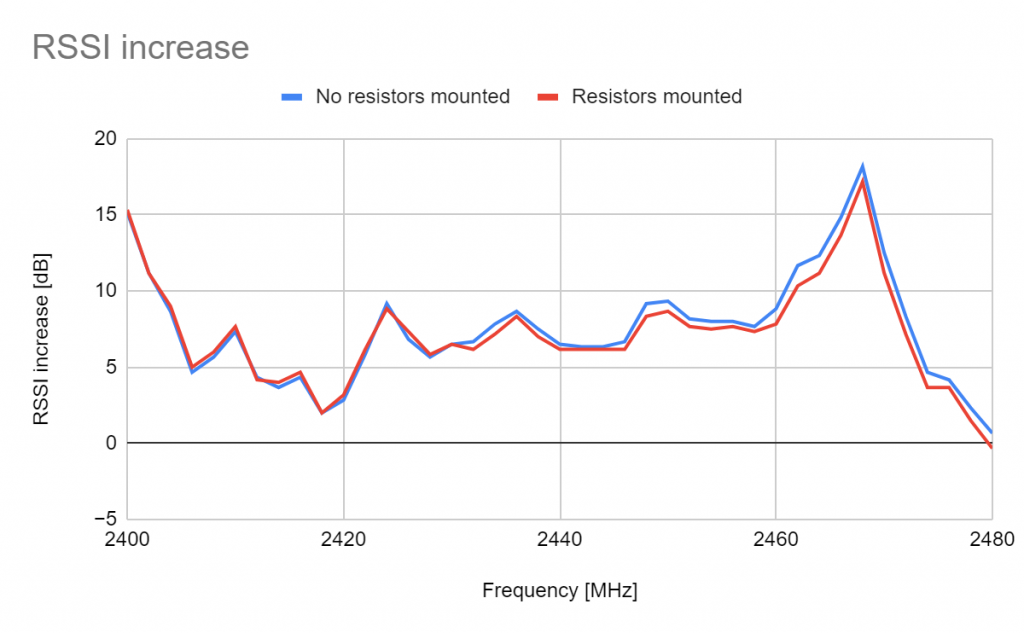
This gives a median and average gain increase over the reference antenna as given by the table below.
| Configuration | Average [dB] | Median [dB] |
| Gain increase, no resistors mounted | 7,540650407 | 7,333333333 |
| Gain increase, resistors mounted | 7,178861789 | 7,166666667 |
If the reference antenna had an average gain of 1 dB, that means that the average maximum gain of the antenna is around 8dBi.
Discussion
With the tests on my roof terrace, I was able to estimate the gain of the manufactured antenna to 8 dBi. However, I would take those measurements with quite a big grain of salt, but I do think it’s neat that such a big gain increase could be measured.
It’s far from the simulated 14 dBi, but some losses are expected. Now the setup, again, is far from ideal and it would be very cool to test this antenna in an antenna chamber, but I have not been able to borrow one, so these measurements will suffice. In reality, I think the gain is somewhere in the middle of the measured result and the simulated result.
One observation pointing in the direction on how poor the test setup actually worked is the RSSI measurements of the two blade antennas. that measurement is all over the place, and as a matter of fact, these are the standard deviations of the three setups:
| Configuration | Standard deviation of RSSI measurements |
| RSSI, blade antennas | 4,980787711 |
| RSSI, one blade antenna, one patch antenna without resistors | 2,876335076 |
| RSSI, one blade antenna, one patch antenna with resistors | 3,263071504 |
I believe that the omnidirectional nature of the blade antennas caused them to pick up a lot of noise and multipath measurements, which in turn was reduced when the directional patch array antenna was measured instead. I didn’t perform measurements between the patch antennas themselves, since it wouldn’t help in measuring the gain, but I would guess that the standard deviation of the RSSI measurements would decrease, as the directionality of the antennas would cause less pickup of multipath signals.
Another observation is the slight decrease in gain on the antenna which had the resistors mounted on the Wilkinson power divider. This is somewhat confusing to me as the resistors would help in reducing reflections by matching all interconnects to 50+0jΩ. On the other hand, the improvement of adding those resistors is probably small all together.
Then there is the final option of me messing up the whole thing and thinking that it worked when it actually didn’t. I would assume that the bandwidth is quite small looking at the S(1,1) parameters, and if the center frequency is shifted due to manufacturing tolerances, the measurements would be out of bounds. A way to measure this would be to test the S(1,1) parameter with a VNA, but again, I don’t have access to one.
Conclusions
I am able to send messages wirelessly at 2.4 GHz with an average 7dB increase with the new patch array antenna, compared to a reference blade antenna.
The simulated gain was 14.84 dBi with a directivity of 19.365 dB, and the measured gain was 8 dBi, but with a suboptimal test setup.
Future work
I have gained a lot of cool ideas from this project, and it was nice going back to RF design for a bit. I would really like to test the parameters of this antenna design in a real lab, not only to see what the actual gain is, but also to see how far off the real antenna is from the simulations. So if anyone tries this either using the design files I’ve provided, or has any other input, please let me know by commenting in the comment section below.
The antenna is quite large, and I think it would be hard to mount this on a small phy-theta robot design as I mentioned in the introduction to this post. So as far as making a smaller version, I think the ruler-antenna is actually a better fit, and to be quite honest I shifted my focus from that project to designing the antenna and all that it includes, as the project went on. This is especially noticeable in the design itself, as I intended to cut out a whole to fit a camera through the center of the antenna, but forgot it as I was simulating.
As far as future antenna designs for me, I would like to try out a modular patch antenna design next. I am however moving, and have a few other ideas I’d like to try out, so it could be a while before I try this.
But the idea is to make one patch antenna design with an inset feed using via and having a micro SMA connector on the secondary side, which connects to a coaxial cable to another PCB. This other PCB could then consist of phase shifter and/or discrete splitters, and the antennas themselves could be steerable physically. I don’t know if this is theoretically possible, as the ground plane would be split between each antenna, and I haven’t really gotten a feeling for how the ground plane interacts between the patches. Moreover, with a modular design you could reconfigure the antennas, and if there is a design error you wouldn’t necessarily need to re-order the whole thing.
Final thoughts
So, I hope you enjoyed reading my lengthy project log, and I would like to stress that this is technically my first antenna design, so I would bet there are wrong assumptions and bad decisions in this post. This project has been funded by myself and made in my own free time, and the intention is to share what I’ve learned and maybe spark some ideas of your own.